Wide band pushpull HF amplifier (1.8 -54 Mhz) - suboptimal performance below 10 Mhz - why ?

Thread Starter

pik

Joined Sep 20, 2018
10
Hello,

I build a wideband HF power amplifier (1.8 - Mhz) inspired from this design published in the ARRL handbook in 2012 (NEW 250 Watt 160 to 6 meter linear amplifier)
Its essentially a 300W HF LDMOS power amplifier using 2 VRF151 powered under 50V, a quite well know and famous RF design in fact.

I am not very experimented with HF amplifiers so I am not sure if the performance that I observe between 2 and 10 Mhz is normal or not. It seems to me the amplifier performs OK between 10 and 50 Mhz, but below 10 Mhz the performance degrades and I am not sure I can do something about it

Description of my set-up:

I wrote "inspired" above because there are differences compared to the design published by the ARRL in 2012:

(a) I do not use source degeneration (0.05 ohm resistor in the source ground path of each VRF151 LDMOS transistors)
(b) The input transformer is a 4:1 TLT instead of a classical tube & sleeve one.

For both the input and outptut TLT transformers I use a Ferrite material 61
(a) For the input TLT transformer I use coax cable of 25 ohms (2X30cm) (ie 25 ohm = SQRT (12.5 ohm *50 ohm) .
(b) For the output TLT I use two coax cable of 50 ohm in parallel in order to reach a Z0 of 25 ohm. The coaxial length of the TLT transformer is also 30cm like for the input one (I just use 4X30cm cables instead of 2X30cm)


On the input side, I have also installed a 1:1 balun ( additional 20cm turns on a additional ferrite toroid made of material 61), so just just like for the output of the RF amplifier.

The problems I see with my set-up

1) Although the signal signal gain below 10 Mhz (VNA test) is as good as above 10 Mhz, the max output power drops very quickly and 2 Mhz I can hardly output more than 100W HF and with a terrible efficiency of 20%. In fact the efficiency is so bad that I am afraid of burning the transistors on the 160m band (1.8 Mhz) band and I do not dare to transmit at more than 80 W HF power)

(I am OK with the performance above 10Mhz, I get a solid 300W HF easily between 10 and 30Mhz and easily 200W HF at 50 Mhz. The efficiency varies between 40% and 60% between 10 and 50 Mhz (10 to 14 amps under 50V), it does not seems to me very good but it is ok with me as the amps works fine)

2) Similar story with the 2nd harmonic: The level of rejection of the second harmonic below 10 Mhz degrades quickly, it is especially bad at 2 Mhz (-15dBc only ) which seems to me incredibly low for a pushpull amplifier

(between 10 and 50 Mhz, the level of rejection of the second harmonic is much better, varying between -40dBc and -50 dBc depending on the freuency)

The advises I am looking for :

- is this performance degradation unavoidable below 10 Mhz ? do I have to accept it ?
- what could explain the performance degradation below 10 Mhz ?

Thanks
Regards
Peter


Mods Note:
The links has copyrights issue, so now we deleted it.
 

cariban

Joined Aug 14, 2018
69
Hello,

I build a wideband HF power amplifier (1.8 - Mhz) inspired from this design published in the ARRL handbook in 2012 (NEW 250 Watt 160 to 6 meter linear amplifier)
Its essentially a 300W HF LDMOS power amplifier using 2 VRF151 powered under 50V, a quite well know and famous RF design in fact.

I am not very experimented with HF amplifiers so I am not sure if the performance that I observe between 2 and 10 Mhz is normal or not. It seems to me the amplifier performs OK between 10 and 50 Mhz, but below 10 Mhz the performance degrades and I am not sure I can do something about it

Description of my set-up:

I wrote "inspired" above because there are differences compared to the design published by the ARRL in 2012:

(a) I do not use source degeneration (0.05 ohm resistor in the source ground path of each VRF151 LDMOS transistors)
(b) The input transformer is a 4:1 TLT instead of a classical tube & sleeve one.

For both the input and outptut TLT transformers I use a Ferrite material 61
(a) For the input TLT transformer I use coax cable of 25 ohms (2X30cm) (ie 25 ohm = SQRT (12.5 ohm *50 ohm) .
(b) For the output TLT I use two coax cable of 50 ohm in parallel in order to reach a Z0 of 25 ohm. The coaxial length of the TLT transformer is also 30cm like for the input one (I just use 4X30cm cables instead of 2X30cm)


On the input side, I have also installed a 1:1 balun ( additional 20cm turns on a additional ferrite toroid made of material 61), so just just like for the output of the RF amplifier.

The problems I see with my set-up

1) Although the signal signal gain below 10 Mhz (VNA test) is as good as above 10 Mhz, the max output power drops very quickly and 2 Mhz I can hardly output more than 100W HF and with a terrible efficiency of 20%. In fact the efficiency is so bad that I am afraid of burning the transistors on the 160m band (1.8 Mhz) band and I do not dare to transmit at more than 80 W HF power)

(I am OK with the performance above 10Mhz, I get a solid 300W HF easily between 10 and 30Mhz and easily 200W HF at 50 Mhz. The efficiency varies between 40% and 60% between 10 and 50 Mhz (10 to 14 amps under 50V), it does not seems to me very good but it is ok with me as the amps works fine)

2) Similar story with the 2nd harmonic: The level of rejection of the second harmonic below 10 Mhz degrades quickly, it is especially bad at 2 Mhz (-15dBc only ) which seems to me incredibly low for a pushpull amplifier

(between 10 and 50 Mhz, the level of rejection of the second harmonic is much better, varying between -40dBc and -50 dBc depending on the freuency)

The advises I am looking for :

- is this performance degradation unavoidable below 10 Mhz ? do I have to accept it ?
- what could explain the performance degradation below 10 Mhz ?

Thanks
Regards
Peter


Mods Note:
The links has copyrights issue, so now we deleted it.
For such high power amplifier, the transistor works at the non-linear range. The gain measured by VNA doesn't reflect the real situation anymore. You must use "load pull" method to measure the impedance. The basic idea of "load pull" is to use tunable capacitor and inductor to obtain the maximum output power. Then use the optimal capacitor/inductor values to calculate the output impedance.

Nevertheless, VNA measurement is still useful since other linear components (for example AC coupling capacitor, transformer) have been evaluated.
 

Thread Starter

pik

Joined Sep 20, 2018
10
For such high power amplifier, the transistor works at the non-linear range. The gain measured by VNA doesn't reflect the real situation anymore. You must use "load pull" method to measure the impedance. The basic idea of "load pull" is to use tunable capacitor and inductor to obtain the maximum output power. Then use the optimal capacitor/inductor values to calculate the output impedance.

Nevertheless, VNA measurement is still useful since other linear components (for example AC coupling capacitor, transformer) have been evaluated.
Dear Cariban,

Thank you for your insight. Indeed I never heard of "Load/Pull" before and will look into this (Google is my friend).

Regards
Peter
 

cariban

Joined Aug 14, 2018
69
Dear Cariban,

Thank you for your insight. Indeed I never heard of "Load/Pull" before and will look into this (Google is my friend).

Regards
Peter
One thing you can test is to increase the input power gradually, then monitoring the output power and calculate the gain at different input power. If the gain decreases with increasing the input power, it is a good indication that you have entered into the non-linear range.
 

Thread Starter

pik

Joined Sep 20, 2018
10
I have done a bit of research on Google on the load-pull concept. What I see is that impedance tuners are mostly used at VHF/UHF/SHF and above frequencies and not really for HF frequencies (so up to 50 Mhz).

Nearly all the high power wideband HF LDMOS amplifiers schematics that I reviewed use a mere wideband 1:4 or 1:9 TLT output transformer with a transformer ratio chosen depending on the target output HF power aimed as well the target operating voltage. Usually a ratio of 1:4 for 300W HF if operating at 50V and a ratio of 1:9 for 800-100W HF if operating at 50V. In other words for HF frequencies is no attempt to find-pout what is the optimal output impedance to present to the two drains of the pushpull LDMOS transistors; the ratio of the output transformer is just chosen so it is possible to reach the target HF output power with the target operating voltage.

Since my amp works ok between 3.5 and roughly 54 Mhz, and shows some degradation of performance in the 160M at 1.8-2 Mhz, I am actually suspecting that the two output/input TLT transformers are no longer doing their job any longer correctly. Following the good old rule, my understanding is that the reactance of the low impedance side of my two 1:4 TLT transformer should be at least +j50 ohms (because 4*12.5 = 50) and for the high impedance side minimum +j200 ohms (4X50=200). I use material ferite 61 to extend the bandwidth of the TLT transformer in the lower part of the HF bands and from what I read material 43 might be preferable for operating at 2 Mhz.

So I will re-test the reactance of my TLT at 2 Mhz and see if it is at least +J50 ohms, if it is less I will try the ferite 43 material instead 61.

Regarding the degradation of the 2nd harmonic suppression below 10 Mhz, since the worse performance is also at 2 Mhz, I am tempted to believe the reason is the same than for the drop of output power; the two TLTs and the two baluns are simply no longer operating optimally at 2Mhz due to the ferite material 61 chosen

feedback and advices welcomed
regards
Peter
 

cariban

Joined Aug 14, 2018
69
I have done a bit of research on Google on the load-pull concept. What I see is that impedance tuners are mostly used at VHF/UHF/SHF and above frequencies and not really for HF frequencies (so up to 50 Mhz).

Nearly all the high power wideband HF LDMOS amplifiers schematics that I reviewed use a mere wideband 1:4 or 1:9 TLT output transformer with a transformer ratio chosen depending on the target output HF power aimed as well the target operating voltage. Usually a ratio of 1:4 for 300W HF if operating at 50V and a ratio of 1:9 for 800-100W HF if operating at 50V. In other words for HF frequencies is no attempt to find-pout what is the optimal output impedance to present to the two drains of the pushpull LDMOS transistors; the ratio of the output transformer is just chosen so it is possible to reach the target HF output power with the target operating voltage.

Since my amp works ok between 3.5 and roughly 54 Mhz, and shows some degradation of performance in the 160M at 1.8-2 Mhz, I am actually suspecting that the two output/input TLT transformers are no longer doing their job any longer correctly. Following the good old rule, my understanding is that the reactance of the low impedance side of my two 1:4 TLT transformer should be at least +j50 ohms (because 4*12.5 = 50) and for the high impedance side minimum +j200 ohms (4X50=200). I use material ferite 61 to extend the bandwidth of the TLT transformer in the lower part of the HF bands and from what I read material 43 might be preferable for operating at 2 Mhz.

So I will re-test the reactance of my TLT at 2 Mhz and see if it is at least +J50 ohms, if it is less I will try the ferite 43 material instead 61.

Regarding the degradation of the 2nd harmonic suppression below 10 Mhz, since the worse performance is also at 2 Mhz, I am tempted to believe the reason is the same than for the drop of output power; the two TLTs and the two baluns are simply no longer operating optimally at 2Mhz due to the ferite material 61 chosen

feedback and advices welcomed
regards
Peter
I also feel that your transformer may get saturated with high current at lower frequency. Please continue to report the progress, I am also curious about the solution. I did design a 10W power amplifier working at UHF band 470 - 862MHz for DVB-T/T2, but no experience with so low frequency. Low frequency amplifier could be another kind of challenge.
 

cariban

Joined Aug 14, 2018
69
Any comments on my measurements


View attachment 161979
Do you have also the measurement of small signal measured by VNA? Also do you have the input impedance plot with output port terminated?
If the difference is big, you should consider to use load-pull method to match the output impedance. Then match the input port as well if needed.
 

Thread Starter

pik

Joined Sep 20, 2018
10
Thank you for your answer. The amp I build is in fact a pre driver (MHW592) ,a driver (2 X MRF134 pushpull) and a Final (2XVRF51). I have indeed measured the small signal gain and the large signal one for each of the 3 stages.

For the pre driver (MHW592 module) there is no difference, the gain is about 35 dB. The compression point is reached around -5 dBm input power and I think this is actually the bottleneck. The large signal gain of the driver and finals (see below) decreased by about 8 dB at 50 Mhz, but I can't compensate the gain drop by increasing the input power as I hit the compression point of the MHW592 module, that's why I think I can not output more than about 150W HF on 50 and 52 Mhz.

For the driver (2XMRF154 pushpull) the small and large signal gains are about the same. It is +15dB except at 50 and 52 Mhz where the gain is in the order of 11dB only (large and small signal). The driver does not a feedback network to flatten the gain, maybe this is part is the problem

For the final stage, there is lno difference of gain between small and large signal either. Here also the gain is relatively flat around 15 dB. I use a negative feedback mechanism between drain and source to flatten the gain. Despite this feedback mechanism, the gain is however about 3-4 dB higher around 18 Mhz than it is at 50 Mhz . I have not measured the input VSWR without the 50 ohm dummy load at the output, will try it.

Regards
Peter
 

cariban

Joined Aug 14, 2018
69
Thank you for your answer. The amp I build is in fact a pre driver (MHW592) ,a driver (2 X MRF134 pushpull) and a Final (2XVRF51). I have indeed measured the small signal gain and the large signal one for each of the 3 stages.

For the pre driver (MHW592 module) there is no difference, the gain is about 35 dB. The compression point is reached around -5 dBm input power and I think this is actually the bottleneck. The large signal gain of the driver and finals (see below) decreased by about 8 dB at 50 Mhz, but I can't compensate the gain drop by increasing the input power as I hit the compression point of the MHW592 module, that's why I think I can not output more than about 150W HF on 50 and 52 Mhz.

For the driver (2XMRF154 pushpull) the small and large signal gains are about the same. It is +15dB except at 50 and 52 Mhz where the gain is in the order of 11dB only (large and small signal). The driver does not a feedback network to flatten the gain, maybe this is part is the problem

For the final stage, there is lno difference of gain between small and large signal either. Here also the gain is relatively flat around 15 dB. I use a negative feedback mechanism between drain and source to flatten the gain. Despite this feedback mechanism, the gain is however about 3-4 dB higher around 18 Mhz than it is at 50 Mhz . I have not measured the input VSWR without the 50 ohm dummy load at the output, will try it.

Regards
Peter
I would think your situation is not so bad. Your pre-amplifier and final stage work well. Actually most people will have the problem at the last stage. Just make the thing more clear, do you have the rated output power of 300W when you measure the last stage?

I just had a quick look at the MRF134 datasheet (you mentioned MRF154 later, I guess it was just a typo). Do you use the reference design shown in Figure 1? Based on Figure 2, you should be able to get 16dB gain at 100MHz. At 50MHz the gain should be even higher. It is actually good news that the gain for small signal and large signal is about the same. Then you may use VNA to measure the small signal s-parameters to find some clue.
 

Thread Starter

pik

Joined Sep 20, 2018
10
I would think your situation is not so bad. Your pre-amplifier and final stage work well. Actually most people will have the problem at the last stage. Just make the thing more clear, do you have the rated output power of 300W when you measure the last stage?

I just had a quick look at the MRF134 datasheet (you mentioned MRF154 later, I guess it was just a typo). Do you use the reference design shown in Figure 1? Based on Figure 2, you should be able to get 16dB gain at 100MHz. At 50MHz the gain should be even higher. It is actually good news that the gain for small signal and large signal is about the same. Then you may use VNA to measure the small signal s-parameters to find some clue.

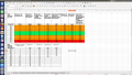
Yes, 300 WHF is actually the output power of the last stage (pushpull VRF151). I get 300 W HF on the last stage except at 50 and 52 Mhz where the max output power ranges between 150 and 200 Mhz (max, see table ). Max output power at 50/52 Mhz varies depending on bias conditions; The higher the bias the higher the gain and the higher the max output. I will nevertheless prepare a summary table with all small and large signal measurements so I see clearly in one go what is the situation for each of the 3 stages.

Yes I use 2XMRF134 not MRF 154, sorry for the typo. I think the reason the measured gain is lower than the one stated in the specifications is simply because the gain stated in the data sheets is the optimal narrow bandwidth one with an output load perfectly (conjugately) matched to the one of the MRF134 so the transfer to the load is optimal. The 3 stages are wide bandwidth ones that are not optimally matched between 2 and 52 Mhz, doing this would allow to have separate tuning circuits for each ham bands which is of course doable but more complex to achieve. The use of wide band TLT transformers is suboptimal from that perspective. I am thinking of replacing the two MRF134 by two MRF136 that can output 15W each (instead of 5W for VRF134) and also have about 3 dB more again; This way I hope I will be able to reach 300 W HF on 50 & 52 Mhz too. I will consider this change after I finalise all my measurement as I want to be sure about what I am doing.

The funny thing is that my initial concern was the performance below 10 Mhz not at 50/52 Mhz. However I discovered that the cheap ham radio power meter that I used initially was actually much too conservative below 5 Mhz and too optimistic above 30 Mhz. The power meter I use nowadays are based on AD8307 and AD8317 chips and are much more accurate. I have calibrated my input/output measurement set up using a reference attenuator and I also ensured that input and output signals measured by the two chips are well below the compression point of the two chips.

Thanks for your advises. I will publish an updated table here with all my measurements.

I am just curious how to understand how to use the pull load method in VHF and UHF, please post the link. It may be usefull for my next amp for the 2M and 70cm band
 

cariban

Joined Aug 14, 2018
69
Yes, 300 WHF is actually the output power of the last stage (pushpull VRF151). I get 300 W HF on the last stage except at 50 and 52 Mhz where the max output power ranges between 150 and 200 Mhz (max, see table ). Max output power at 50/52 Mhz varies depending on bias conditions; The higher the bias the higher the gain and the higher the max output. I will nevertheless prepare a summary table with all small and large signal measurements so I see clearly in one go what is the situation for each of the 3 stages.

Yes I use 2XMRF134 not MRF 154, sorry for the typo. I think the reason the measured gain is lower than the one stated in the specifications is simply because the gain stated in the data sheets is the optimal narrow bandwidth one with an output load perfectly (conjugately) matched to the one of the MRF134 so the transfer to the load is optimal. The 3 stages are wide bandwidth ones that are not optimally matched between 2 and 52 Mhz, doing this would allow to have separate tuning circuits for each ham bands which is of course doable but more complex to achieve. The use of wide band TLT transformers is suboptimal from that perspective. I am thinking of replacing the two MRF134 by two MRF136 that can output 15W each (instead of 5W for VRF134) and also have about 3 dB more again; This way I hope I will be able to reach 300 W HF on 50 & 52 Mhz too. I will consider this change after I finalise all my measurement as I want to be sure about what I am doing.

The funny thing is that my initial concern was the performance below 10 Mhz not at 50/52 Mhz. However I discovered that the cheap ham radio power meter that I used initially was actually much too conservative below 5 Mhz and too optimistic above 30 Mhz. The power meter I use nowadays are based on AD8307 and AD8317 chips and are much more accurate. I have calibrated my input/output measurement set up using a reference attenuator and I also ensured that input and output signals measured by the two chips are well below the compression point of the two chips.

Thanks for your advises. I will publish an updated table here with all my measurements.

I am just curious how to understand how to use the pull load method in VHF and UHF, please post the link. It may be usefull for my next amp for the 2M and 70cm band
Good summary. I also think you may need to use more powerful amplifier for the middle stage since 5W is just enough to get 300W final output. The margin is too small.

I don't quite agree with your point:
"I think the reason the measured gain is lower than the one stated in the specifications is simply because the gain stated in the data sheets is the optimal narrow bandwidth one with an output load perfectly (conjugately) matched to the one of the MRF134 so the transfer to the load is optimal."
If both input and output ports are perfectly conjugate matched, we will obtain so called "maximum available gain". Actually this plot is shown in Figure 11 in the datasheet. Of course in Figure 11 the Id = 100mA, and this may lead to higher gain, but the gain should not be much higher that Id = 50mA. From Figure 11, I feel that it may be possible to get higher and flatter gain by playing the matching network and feedback network.
 
Last edited:

Thread Starter

pik

Joined Sep 20, 2018
10
Ok so I re-did all my measurement, stage by stage in a systematic way and I finally identfied the problem with my amplifier. It was actually much simpler than what I thought.

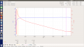
The pre-driver (MHW592) is the Culprit. This module is supposed to provide 35 dB gain and deliver output power of about 30dbm over a flat bandwidth ranging from from 500 Khz to 250 Mhz. Unfortunatelly the model that I bought in China via Aliexpress only partially meet these specifications; the gain is only 22dB at 2 Mhz, stays below 30 dB untill 10 Mhz and it gradually increases from 30 dB at 10 Mhz to 35 dB at 50 Mhz. I suspect it is a counterfeited module or a module that did not pass the QC tests. Anyway it explains why I had such a huge difference of gain between lower and higher HF bands. It had nothing to do with the quality of my output transformers or the matching networks (or the lack thereof), it was a poor quality component.

I have measured the gain of the driver (pushpull MRF154) and it is nearly flat from 2 to 52 Mhz, it varies between 13dB and 18 dB depending on bias conditions
I have measured the gain of the final stage (pushpull VRF151) and with a some drain source feedback it is possible to get a flat 15 dB gain between 2 and 52 Mhz too. Without any drain source feedback network, the gain reaches 22dB at 2 Mhz down to 15 dB at 52 Mhz (each VRF151 is biased close to 400 ma).

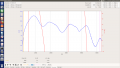
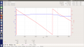
At the moment, I am using the final stage (pushpull VRF151) without any feedback network in order to partially compensate the poor performance of the MHW592 below 10 Mhz. As a result I get a very bumpy gain curve (see below) and I have to bias the driver and final transistors to quite a high quiescent current , but it works for me as I can output my target power of 300 W HF from 2 to 52 Mhz with an IMD3 in the order of -30dBc.. I just have to pay attention not to overdrive the finals on some frequencies as the gain of this amplifier is very HIGH....

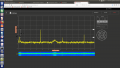
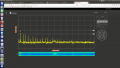
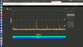
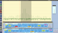
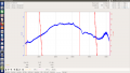
The two pictures below show the gain of the amplifier and of the sub-optimal MHW592 module bought in China. For the amplifier, add 65 dB gain to the value showed by the curve to get the real gain (65 dB is the value of the atenuator used).

This solve the mystery of poor performance on lower HF bands, and along the way, I learned to make accurate rf power measurements using power meters and my spectrum analyzer.
 

Attachments

cariban

Joined Aug 14, 2018
69
Ok so I re-did all my measurement, stage by stage in a systematic way and I finally identfied the problem with my amplifier. It was actually much simpler than what I thought.

The pre-driver (MHW592) is the Culprit. This module is supposed to provide 35 dB gain and deliver output power of about 30dbm over a flat bandwidth ranging from from 500 Khz to 250 Mhz. Unfortunatelly the model that I bought in China via Aliexpress only partially meet these specifications; the gain is only 22dB at 2 Mhz, stays below 30 dB untill 10 Mhz and it gradually increases from 30 dB at 10 Mhz to 35 dB at 50 Mhz. I suspect it is a counterfeited module or a module that did not pass the QC tests. Anyway it explains why I had such a huge difference of gain between lower and higher HF bands. It had nothing to do with the quality of my output transformers or the matching networks (or the lack thereof), it was a poor quality component.

I have measured the gain of the driver (pushpull MRF154) and it is nearly flat from 2 to 52 Mhz, it varies between 13dB and 18 dB depending on bias conditions
I have measured the gain of the final stage (pushpull VRF151) and with a some drain source feedback it is possible to get a flat 15 dB gain between 2 and 52 Mhz too. Without any drain source feedback network, the gain reaches 22dB at 2 Mhz down to 15 dB at 52 Mhz (each VRF151 is biased close to 400 ma).

At the moment, I am using the final stage (pushpull VRF151) without any feedback network in order to partially compensate the poor performance of the MHW592 below 10 Mhz. As a result I get a very bumpy gain curve (see below) and I have to bias the driver and final transistors to quite a high quiescent current , but it works for me as I can output my target power of 300 W HF from 2 to 52 Mhz with an IMD3 in the order of -30dBc.. I just have to pay attention not to overdrive the finals on some frequencies as the gain of this amplifier is very HIGH....

The two pictures below show the gain of the amplifier and of the sub-optimal MHW592 module bought in China. For the amplifier, add 65 dB gain to the value showed by the curve to get the real gain (65 dB is the value of the atenuator used).

This solve the mystery of poor performance on lower HF bands, and along the way, I learned to make accurate rf power measurements using power meters and my spectrum analyzer.
Congratulations with the progress! I also bought a lot of stuff from Aliexpress, but not for serious product like this.
 

Thread Starter

pik

Joined Sep 20, 2018
10
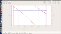
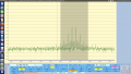
Replaced the problematic MHW592 module by a CA2818 that I had available in my drawer. The gain is much lesser than the MHW592, only 17 to 18 dB but is very flat from 1 Mhz to 60 Mhz. As a result I reintroduced some gate source feedback network in the final stage and the total gain of the amplifier is much less bumby (see picture). The total gain varies between 48 and 51 dB, during my test I could easily reach 300 W HF from 2 to 52 Mhz with less than 10 dBm input power.

Next step is tp finalise the 7 order low pass Cauer filter that I built in order to get rid of harmonics. I also want to try to optimise the feedback network to reach an even flatter gain in the order of 50 dB with no more than 1dB difference between 2 and 52 Mhz.

upload_2018-11-7_2-17-8.png
 

cariban

Joined Aug 14, 2018
69
Replaced the problematic MHW592 module by a CA2818 that I had available in my drawer. The gain is much lesser than the MHW592, only 17 to 18 dB but is very flat from 1 Mhz to 60 Mhz. As a result I reintroduced some gate source feedback network in the final stage and the total gain of the amplifier is much less bumby (see picture). The total gain varies between 48 and 51 dB, during my test I could easily reach 300 W HF from 2 to 52 Mhz with less than 10 dBm input power.

Next step is tp finalise the 7 order low pass Cauer filter that I built in order to get rid of harmonics. I also want to try to optimise the feedback network to reach an even flatter gain in the order of 50 dB with no more than 1dB difference between 2 and 52 Mhz.

View attachment 163262
Good progress! BTW, the harmonics is still bad at some frequency band?
 
Top