Why wont these transistors of my differential pair go into saturation no matter what I do

Thread Starter

arhzz1

Joined Oct 21, 2020
61
Hello! (quick disclaimer all of this is very new to me so if my questions sounds stupid I apologize in advance)

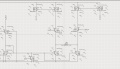
Consider this differential pair 1744572390736.png


I am using diode connected PMOS loads and external biasing done via the Ibias pin; I have one degeneration resistor and M12 and M13 are susposed to be a part of an enable circuit (it is to the left and connected to the differential pair but for the sake of readibilty I didnt post it). I am feeding Vin and Vip with an external single ended to differental circuit that looks like this;

1744572519488.png

And last but not least this is my test bench;


In my Ngspice terminal I have saved the small signal values of every transistor (gm,ids vgs,fug,cgg,vds..) and in my control block I am trying for one; to find my gm/id of the 2 NMOS transistors that have Vip and Vin attached to them so that with, that gm/id value i can get a realisitc value for my Ibias (i assummed that gm/id = 12 but my professor said this could be off). and after that I am trying to find my Gm in my input range from -1.2 to 1.2 and plot it out. 1744573083296.png
Now as for my understanding my goal firstly should be, that all of my transistors (expect my enable transistors since I want them to be switches) should be in saturation. And here comes the problem;

1744573132929.png
M6 and M2 are not in saturation, while M13 is;

I have tried everything I can think of to get M6 and M2 into saturation but I just cant; tried changing W and L, didnt help, tried increasing Ibias didnt help. Varied Rs from 1ohm to 1MOhm, didnt help, tried removing M13 didnt help. No matter what I do they wont be saturated so my gm plot is way off.

Any advice? What am I missing. Thanks in advance!
 

Attachments

Papabravo

Joined Feb 24, 2006
22,058
I believe the circuit configuration of a differential amplifier prevents that. Going into either saturation or cutoff would clip the output at the rails which is not something useful for an amplifer to do since that essentially means it stops being an amplifier. I'm curious about why you would not know or expect this to be the case. What are you actually trying to do?
 

BobTPH

Joined Jun 5, 2013
11,463
Why are you trying to use a differential pair for switching? That is no something I have ever heard of. What is special about your project that prevents you from using the trivial MOSFET switching configuration?
 

Thread Starter

arhzz1

Joined Oct 21, 2020
61
I believe the circuit configuration of a differential amplifier prevents that. Going into either saturation or cutoff would clip the output at the rails which is not something useful for an amplifer to do since that essentially means it stops being an amplifier. I'm curious about why you would not know or expect this to be the case. What are you actually trying to do?
Okay here is what I am actually trying to do;build low power general-purpose transconductor (Gm-Cell) that can be a building block for a Gm-C filter.(the filter is not my concern that is made by another student on the project)

Now this is my core circuit(the circuit I posted in my #1) and for that circuit I need to run following simulations in Xschem; dc (input range) ac(bandwidth) tran(linearity) noise(input noise)


Now this circuit specifications regarding bandwith, input noise etc...and the first thing I needed to find was Ibias range so that it matches my Gmeff range of 1uS to 10uS; for that I was given these 2 equations;

1744582473000.png1744582482030.png
(These are from the Tony Charusone book); where Vimax is my input voltage Vi is Ibias;

Now i replaced the small signal transcondutance with gm/Id* Id (where Id is Ibias) and I assumed moderate inversion so gm/id around 12

Now I used these 2 formulas to derive my equation for an Ibias range and the equation was correct (according to my professor)

Now I need to run all of the above simulations for an gmeff 2uS and the matching Ibias I got from these 2 equations; So that is a short TLDR of what my task is and how I ended up here;

What I am actually trying to do is run the dc simulation and expect an gm plot in Xschem that looks kind of like this 1744582768430.png

(from the Razhavi book)

Ideally my professor said I want it to be completly flat at the top in between -Vin and Vin but that is if we are aiming for perfection;

Now here is what I get when I try to simulate the circuit I have posted 1744582961602.png

Not quite the same;

So my professor suggested that I "add small signal parameters in my subcircuit so that I can see if the transistors are in saturation, and see if my assumption of my gm/id was correct" ; hence my assumption that all transistors need to be in saturation

So I am not trying to build a switch using a differential pair; hopefully its clearer now, excuse the confusion.
 

Papabravo

Joined Feb 24, 2006
22,058
Okay here is what I am actually trying to do;build low power general-purpose transconductor (Gm-Cell) that can be a building block for a Gm-C filter.(the filter is not my concern that is made by another student on the project)

Now this is my core circuit(the circuit I posted in my #1) and for that circuit I need to run following simulations in Xschem; dc (input range) ac(bandwidth) tran(linearity) noise(input noise)


Now this circuit specifications regarding bandwith, input noise etc...and the first thing I needed to find was Ibias range so that it matches my Gmeff range of 1uS to 10uS; for that I was given these 2 equations;

View attachment 346850View attachment 346851
(These are from the Tony Charusone book); where Vimax is my input voltage Vi is Ibias;

Now i replaced the small signal transcondutance with gm/Id* Id (where Id is Ibias) and I assumed moderate inversion so gm/id around 12

Now I used these 2 formulas to derive my equation for an Ibias range and the equation was correct (according to my professor)

Now I need to run all of the above simulations for an gmeff 2uS and the matching Ibias I got from these 2 equations; So that is a short TLDR of what my task is and how I ended up here;

What I am actually trying to do is run the dc simulation and expect an gm plot in Xschem that looks kind of like this View attachment 346853

(from the Razhavi book)

Ideally my professor said I want it to be completly flat at the top in between -Vin and Vin but that is if we are aiming for perfection;

Now here is what I get when I try to simulate the circuit I have posted View attachment 346855

Not quite the same;

So my professor suggested that I "add small signal parameters in my subcircuit so that I can see if the transistors are in saturation, and see if my assumption of my gm/id was correct" ; hence my assumption that all transistors need to be in saturation

So I am not trying to build a switch using a differential pair; hopefully its clearer now, excuse the confusion.
Nobody ever said you were trying to build a switch, but you certainly have not built a differential amplifier. What you have seems to be the equivalent of a notch filter where you get no output for small differential inputs. You need to go back to first principles and design an actual differential amplifier. You should be prepared to throw your first design away because you usually end up doing that anyway.

ETA: The following paper may be of interest because it has graphs that look superficially similar to the ones you are presenting.
design-of-highly-linear-cmos-gmcell-for-continuous-time-filter-applications_March_2013_3569094513_0214693.pdf

ETA2: I believe that a Gm Cell on a die is roughly equivalent a discrete OTA (Operation Transconductance Amplifier). The output of those amplifiers is meaningless without a suitable output impedance to work into. Does your Gm Cell have the same requirement?
 
Last edited:

Thread Starter

arhzz1

Joined Oct 21, 2020
61
Nobody ever said you were trying to build a switch, but you certainly have not built a differential amplifier. What you have seems to be the equivalent of a notch filter where you get no output for small differential inputs. You need to go back to first principles and design an actual differential amplifier. You should be prepared to throw your first design away because you usually end up doing that anyway.

ETA: The following paper may be of interest because it has graphs that look superficially similar to the ones you are presenting.
design-of-highly-linear-cmos-gmcell-for-continuous-time-filter-applications_March_2013_3569094513_0214693.pdf

ETA2: I believe that a Gm Cell on a die is roughly equivalent a discrete OTA (Operation Transconductance Amplifier). The output of those amplifiers is meaningless without a suitable output impedance to work into. Does your Gm Cell have the same requirement?
That is also a question that should be answered; it says I should simulate the circuit I posted in #1 and the question is ; "How should the circuit be loaded" ?

I went into it with the idea of putting 0 resitors first ( I have 0V sources ) just to verify the circuit operation, and considered adding loads later.

For the bandwith simulation, I am given a capacitance load I should use and check if the bandwidth fullfills the requirements with the given load.


With the switch I was refering to the anwer of BobPTH in#3; And for the design, here is the kicker I was actually given how the circuit (not dimensions) looks like; For reference; 1744636217560.png

This is my core circuit without biasing and enable circuit; I was susposed to figure that on my own. Hence my circuit; (enable part is not there but my professor said it looked okay). So I have no problem that my original design is trash, but it is not really my design. Any advice? Maybe talk to my professor or?

Thank you for the paper I will read through it, maybe some things become more clear.
 
Top