Why we need Read bit in SPI and what is a dummy byte ?

Thread Starter

Xenon02

Joined Feb 24, 2021
504
If the master wants to send data to the slave, the master loads the shift register and sends the data.
Ok quite similar to what I said.


If the master wants to receive data from the slave after the initial transmission, the master sends data to the slave (which could be a command that expects n bytes to be returned). The master then sends n bytes and receives n bytes from the slave.
Well it sends the n byte to the slave to say "hey I want to read what you have in the device register"and at the same time slave sends the dummy byte as I understood. After that the slave loads the register like in the first quote (instead of master of course), and then slave sends to master and master sends also to the slave the dummy data.

That's what I understood with the dummy data. And I read that the dummy data is 0x00 or 0xFF.
So most likely the scenerio nr.2 is correct I guess. If not then why ?

Or what is wrong with my example ? Because I want/need the example to understand it with bits/bytes.
 

nsaspook

Joined Aug 27, 2009
16,426
What you need to send per transaction and what you get per transaction (what's in the client SPI buffer to send to the master per transaction) is up the the client protocol.
This is for a SPI connected IMU device client. https://www.murata.com/en-us/products/sensor/accel/overview/lineup/sca3300

1698961857089.png
https://www.mouser.com/catalog/specsheets/Murata_datasheet_sca3300_d01.pdf
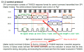
5.1.2 Protocol The SPI is a 32-bit 4-wire slave configured bus. Off-frame protocol is used so each transfer consists of two phases. A response to the request is sent within next request frame. The response concurrent to the request contains the data requested by the previous command. The first bit in a sequence is an MSB.
1698962090724.png
1698962219196.png
C:
    /* Device commands and response */
#define SCA3300_REG_WHOAMI    0x10
#define SCA3300_WHOAMI_ID    0x51
#define SCA3300_WHOAMI_ID_SCL    0xC1
#define SCA3300_WHOAMI_32B    0x40000091
#define SCA3300_SWRESET_32B    0xB4002098
#define SCA3300_RS_32B        0x180000E5
#define    SCA3300_ACC_X_32B    0x040000F7
#define    SCA3300_ACC_Y_32B    0x080000FD
#define    SCA3300_ACC_Z_32B    0x0C0000FB
#define SCA3300_TEMP_32B    0x140000EF
#define SCA3300_MODE1        0xB400001F  
#define SCA3300_MODE2        0xB4000102  
#define SCA3300_MODE3        0xB4000225
#define SCA3300_MODE4        0xB4000338
#define SCL3300_MODE1        0xB400001F
#define SCL3300_MODE2        0xB4000102
#define SCL3300_MODE3        0xB4000225
#define SCL3300_MODE4        0xB4000338
#define SCL3300_ANGLE        0xB0001F6F
#define SCL3300_E_FLAG1        0x1C0000E3
#define SCL3300_E_FLAG2        0x200000C1
#define    SCL3300_ANG_X_32B    0x240000C7
#define    SCL3300_ANG_Y_32B    0x280000CD
#define    SCL3300_ANG_Z_32B    0x2C0000CB
#define SCA3300_BANK0           0xFC000073
#define SCA3300_BANK1           0xFC00016E
#define SCA3300_SERIAL1         0x640000A7
#define SCA3300_SERIAL2         0x680000AD  

#define SCA3300_CHIP_ID_DELAY        10000    // ID command repeat delays in usec
#define SCA3300_CHIP_SWR_DELAY        10000    // chip software reset delay
#define SCA3300_CHIP_MODE_DELAY        100000    // chip G mode setup delay
#define SCA3300_CHIP_CS_DELAY        11    // CS high min duration between toggles
#define SCA3300_CHIP_BTYES_PER_SPI    4    // 32-bit transfers, 4 bytes

/*
* talk to the IMU via the SPI port
*/
bool sca3300_imu_transfer(imu_cmd_t * imu, uint32_t data)
{
    imu_cs(imu); // select IMU on SPI bus after required delay between SPI requests
    imu->tbuf32[SCA3300_TRM] = data; // data request command as 32-bit word with CRC
    SPI2_WriteRead(imu->tbuf32, SCA3300_CHIP_BTYES_PER_SPI, imu->rbuf32, SCA3300_CHIP_BTYES_PER_SPI);
    StartTimer(TMR_CS, SCA3300_CHIP_CS_DELAY); // milliseconds
    while (imu->run) { // wait until data has left the SPI buffer, run flag is set in SPI interrupt ISR
        if (TimerDone(TMR_CS)) {
            return false;
        }
    };

    return true;
}
The SPI transfer function, two memory buffers tbuf32, rbuf32 and lengths SCA3300_CHIP_BTYES_PER_SPI is 4 bytes
C:
/*
* Read raw ACCEL data from the chip using SPI
* check all returned SPI data for proper CRC
* Off-frame protocol is used so each
* transfer consists of two phases. A response to the request is sent within next request
* frame. The response concurrent to the request contains the data requested by the
* previous command.
* ~160us runtime per full data update
*/
bool sca3300_getdata(void * imup)
{
    imu_cmd_t * imu = imup;

    if (imu) {
        if (!imu->run) {
            // junk first response
            imu->crc_error = false; // reset CRC checking flag
            // dummy result return on first command

            sca3300_imu_transfer(imu, SCA3300_ACC_X_32B);
            sca3300_check_crc(imu, SCA3300_REC); // check dummy for CRC error

            sca3300_imu_transfer(imu, SCA3300_ACC_Y_32B);
            if (sca3300_check_crc(imu, SCA3300_REC)) {
                sdata.scan.channels[SCA3300_ACC_X] = ((imu->rbuf32[SCA3300_REC] >> 8)&0xffff); // X data
            };

            sca3300_imu_transfer(imu, SCA3300_ACC_Z_32B);
            if (sca3300_check_crc(imu, SCA3300_REC)) {
                sdata.scan.channels[SCA3300_ACC_Y] = ((imu->rbuf32[SCA3300_REC] >> 8)&0xffff); // Y data
            };

            sca3300_imu_transfer(imu, SCA3300_TEMP_32B);
            if (sca3300_check_crc(imu, SCA3300_REC)) {
                sdata.scan.channels[SCA3300_ACC_Z] = ((imu->rbuf32[SCA3300_REC] >> 8)&0xffff); // Z data
            };

            sca3300_imu_transfer(imu, SCA3300_RS_32B);
            if (sca3300_check_crc(imu, SCA3300_REC)) {
                sdata.scan.channels[SCA3300_TEMP] = ((imu->rbuf32[SCA3300_REC] >> 8)&0xffff); // Z data
            };

            sca3300_imu_transfer(imu, SCA3300_RS_32B);
            if (sca3300_check_crc(imu, SCA3300_REC)) {
                sdata.scan.ret_status = ((imu->rbuf32[SCA3300_REC] >> 8)&0xffff); // return status data
            };

            if (imu->device == IMU_SCL3300) { // we also need angles data
                sca3300_imu_transfer(imu, SCL3300_ANG_X_32B);
                sca3300_check_crc(imu, SCA3300_REC); // check dummy for CRC error

                sca3300_imu_transfer(imu, SCL3300_ANG_Y_32B);
                if (sca3300_check_crc(imu, SCA3300_REC)) {
                    sdata.scan.channels[SCL3300_ANG_X] = ((imu->rbuf32[SCA3300_REC] >> 8)&0xffff); // X data
                };

                sca3300_imu_transfer(imu, SCL3300_ANG_Z_32B);
                if (sca3300_check_crc(imu, SCA3300_REC)) {
                    sdata.scan.channels[SCL3300_ANG_Y] = ((imu->rbuf32[SCA3300_REC] >> 8)&0xffff); // Y data
                };

                sca3300_imu_transfer(imu, SCA3300_RS_32B);
                if (sca3300_check_crc(imu, SCA3300_REC)) {
                    sdata.scan.channels[SCL3300_ANG_Z] = ((imu->rbuf32[SCA3300_REC] >> 8)&0xffff); // Z data
                };
            }

#ifdef __32MK0512MCJ048__
            sdata.scan.ts = TMR9_CounterGet(); // load a clock time-stamp from timer9 32-bit counter, frequency 234,375KHz, 266.66 min roll-over
#endif
#ifdef __32MZ1025W104132__
            sdata.scan.ts = TMR2_CounterGet(); // load a clock time-stamp from timer9 32-bit counter, frequency 234,375KHz, 266.66 min roll-over
#endif
        }
        return imu->online;
    } else {
        return false;
    }
}
A full IMU data update from the IMU. For starters I request X, and get dummy data first. When I request Y, I get X data and so forth.

All we know for sure with any SPI device is that the SPI hardware, on the master and slave, exchange buffers when the SCK clocks start when properly setup and sequenced.
 

Thread Starter

Xenon02

Joined Feb 24, 2021
504
This :
1698963481452.png

And this :

1698963535753.png

Must work like that.

So I still have two questions which weren't answered and I would like it to be answered.

1. Is my scenario nr 2 correct from post nr. 12 ?
2. The dummy byte is 0x00 or 0xFF and according to your picture :

1698963481452.png
Here 3 time is sent data yes ?
so now Slave register has some random stuff like (01000000) and Master has (01010000) at the end of transaction Slave has (01010000) and Master has (01000000) Master wants to send more data so it overwrites (with 01010100) the Master and the Slave is cleared to 0x00 to send dummy byte and the cycle repeats ??? Which is that The slave has (01010100) and the Master has (00000000) and again, read the registers, clear the slave, overwrite the master and again. If we want to read from register then the Master has the dummy byte


I'm getting mixed with the moment when I don't know what is wrong with the specifics I say. I don't know if I am partly correct or not.
 

nsaspook

Joined Aug 27, 2009
16,426
You're asking a device specific protocol question of some devices data interchange, not a generic SPI question, YMMV. For the SCA3300, you need to send an extra dummy (of some sort) command to clock response 3 into the master receive buffer from the slave transmit buffer. What's in the slave transmit buffer after that depends on what you used as the dummy command to get response 3.
 

Thread Starter

Xenon02

Joined Feb 24, 2021
504
You're asking a device specific protocol question of some devices data interchange, not a generic SPI question, YMMV. For the SCA3300, you need to send an extra dummy command to clock response 3 into the master receive buffer form the slave transmit buffer. What's in the slave buffer after that depends on what you used as the dummy command to get response 3.
I don't know exactly how the SPI protocol works, if what I said is specific to a device then I don't exactly understand how this dummy works and why it exist. Why it needs dummy data like that ?

I'll try to be more specific.
After knowing that when receiving the slave data, the master must send something right ? No matter what the device is master must send something, so I thought that the master sends the dummy byte, and opposite if the master sends something then slave sends the dummy byte. Because that was logical to me.

Or is it that it can be like in scenario 1 that if master sends something to slave then slave doesn't send a dummy byte but old stuff to the master and master just overwrites it if it's necessery.

Or in fact it depends, because both first and second scenerio can be correct ??? I'm lost here to be honest. Because I don't really know from my example if the registers is cleared to (0x00 - dummy byte) or just stays as it is and sends the old data back to master and slave receives new data.

Sorry for problem but this is confusing. Even though SPI isn't complex in itself because we use SPI_Transmit and SPI_Receive.

Or is in my first post code has any dummy byte ?

Like here as well :
1698965189826.png
The Master receives what slave gives him but what slave receives ? Dummy byte ? I'm a confused.
 

nsaspook

Joined Aug 27, 2009
16,426
The first, second and more scenario's can be correct. It's all specified by the device datasheet.

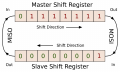
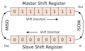
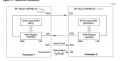
(SPI) at the hardware level is not really a protocol, it's just hardware, that in the simplest implementation can be a shift register interface between to remote shift registers.
1698965591928.png
If you understand this, then you understand how SPI works. At the next level are SPI module hardware implementation details to make the simple shift register interface better but on the actual wire it's the same with simple 4-wire SPI.

What happens when they actually exchange data is device dependent (extra true with multi-byte command/response sequences) at the next level (SPI hardware to program API routines). With multi-byte sequences the first few bits of MOSI first byte could decide what's on the wire with byte 2 coming from MISO, byte 3, etc ...
 

Thread Starter

Xenon02

Joined Feb 24, 2021
504
The first, second and more scenario's can be correct. It's all specified by the device datasheet.
So I understand I wasn't really that wrong ?


SPI) at the hardware level is not really a protocol, it's just hardware, that in the simplest implementation can be a shift register interface between to remote shift registers.
1698965591928.png

If you understand this, then you how SPI works.
Yes I understood that SPI is like in the picture, two shifting registers that sends data to each other. So this is how SPI just works.

So the implementations like clearing the slave or master to have a dummy byte or the scenario which the only thing is made is overwriting the master or slave and the code/implementation decides what happens to it.

I was very confused at some point, but maybe I get it somehow. So dummy bytes are sometimes required and sended manually or implemented already in the device. Although reseting the Master register in SPI could indicate that the SPI works like that because usually the external devices have some kind of implementation. Which means that Master has different implementation of SPI and Slave also has different implementation. Hmmm how do they work though.

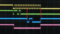
I've found this example :

1698968034716.png

the green one is the MOSI and the blue one is MISO, purple is CS and yellow i SCLK.

So Master sends the data to Slave which is 11010000 and Slave sends the dummy byte which is 11111111, So now master has 111111111 and Slave has 11010000. Then Master overwrites it with 00000000 (but it didn't show that it received 11111111) and Slave also overwrites his register with new data which is 01100000.

So it indicates that when Master wants to read it sends the dummy byte everytime and if Master want to write then Slayer sends its dummy byte everytime it master write something.

So it indicates that both master and slave are using dummy bytes in this example. So I guess it doesn't work in every SPI it is not also a part of SPI that master when reads sends dummy byte and when slayer reads is also sends dummy byte ? It can work like in my second scenerio which Master register doesn't change 11111111 into 00000000 but just stays with 11111111 ?
And the same goes with Slave ?

This is kinda mixing because then we have two different implementation which can be conflicting. Like your exaple where dummy byte is needed but what if it's send by accident because your device uses dummy byte when it read from slayer.
You know what I mean ?

It could also mean that my STM32 SPI works that everytime it reads it sends the dummy byte, but the slave can work differently because it is a different device.

Because if the SPI itself is just a two registers is ok but the protocoles are different so how STM32 can adjust to this ? Or is there a protocol standard how the data is readed from SPI and what a device must send through SPI ?
I know SPI must send and receive at the same time so either they are sending the dummy byte or something else but this dummy byte by default can be weird when it is needed in device and we put it manually but our device makes another dummy byte by accident. So you know, sorry ;<
 
Last edited:

nsaspook

Joined Aug 27, 2009
16,426
SPI is a dumb wire interface.

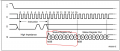
Your image is looking at the wire. It's only shows what's on the wire, your interpretation of what that means, at the device level, is higher level device dependent for dummies or what is a dummy, that maybe needs to be send or are received. Your program tells the STM32 what to do with the data once it's signaled the exchange is complete.. The STM32 hardware interfaces with the shift register interface, the upper levels of the program code handle device protocol issues and requirements.
1698971490383.png
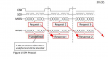
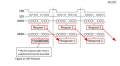
Basic SPI Frame

The CS/SS can not only start a SPI frame (data and clocks that happen during CS/SS active assertion) it can also enable a slave device functions like an ADC conversion that can be clocked out during the same frame. There are no standard SPI data protocols at the device function register level.
 

Thread Starter

Xenon02

Joined Feb 24, 2021
504
Your image is looking at the wire. It's only shows what's on the wire, your interpretation of what that means, at the device level, is higher level device dependent for dummies or what is a dummy, that maybe needs to be send or are received. Your program tells the STM32 what to do with the data once it's signaled the exchange is complete.. The STM32 hardware interfaces with the shift register interface, the upper levels of the program code handle device protocol issues and requirements.
Okay hmmm

So as I understood so on my example the master that sends 00000000 doesn't have to be a dummy ? So I guess the device that takes this signal 00000000 ignores it because it was sent while Slave was sending it, but this dummy is important if the user sends it by himselfs and not generated by the device.

I just wondered because what STM will do with Master and what a device will do with Slaver are two different things, even though they have the same hardware which can be a register shifter, but they have different intepretation or have a protocol to for example sends dummies while doing something but the Master can do the same and send it by accident and what then ?

I also understand that I correctly analized the example ?


Your image is looking at the wire.
Yea forgot, so I think the master indeed received from slave this 11111111 and just overwrited it with 00000000 because it is reading from slave so it must send a dummie. Or I think this is a dummie, at least that's what people say what is the value of a dummie byte.


your interpretation of what that means, at the device level, is higher level device dependent for dummies or what is a dummy, that maybe needs to be send or are received. Your program tells the STM32 what to do with the data once it's signaled the exchange is complete..
But STM can have a different behavior what to do when for example he reads from slave, let's say when he reads he sends 00000000 (because something must be sent to slave right ?), and slave when he reads he doesn't send dummies like 11111111 or 00000000. But I guess even if dummies are required from this device then if he sends data he ignores the new data he received while sending (which is the dummie sent by Master while he was reading from Slave (reading mode))


Do you think I grasped the idea how it looks like ?
 

MrChips

Joined Oct 2, 2009
35,012
You are making a mistake to think that 00000000 and 11111111 are dummy data.
00000000 has as much significance as 11111111 and any of the other 254 possibilities of 8-bit zeros and ones.
 

tumbleweed

Joined Jun 27, 2023
19
SPI isn't complex in itself because we use SPI_Transmit and SPI_Receive.
That's part of the problem. There is no individual "SPI_Transmit" or "SPI_Receive" function.
SPI is an "exchange" protocol... every time you transmit a byte you get a byte back at the same time.

The bytes exchanged may or may not be actual valid data... they could just be "placeholders" to get a byte transferred.
On the master side you typically send "dummy" bytes so that you can get response bytes back from the slave,
and on the slave side data it sends is usually only valid after some specific sequence of bytes received.

That's all up to the individual device protocol, so it can be different every time.
 

Thread Starter

Xenon02

Joined Feb 24, 2021
504
it's better but the only way to gain practical experience/intuition is to build things and to lose a little hair until it works correctly.
I've send what I did in my SPI (post nr .1) so I tried to understand from my example what it does. My master sent 10001111 and what slave then sent ? After that I used the SPI_Receive and then the Slave sends data which should be 11010100 but master must send something so I was wondering if that was the case and what it was sending then what are the possibilitys.

Also I was having a problem understanding how 2 devices are working if they have different protocoles like I've mentioned with sending 00000000 to the slave while master is reading from slave, the slave can interprate it wrongly. But if the dummy byte must be send manually then maybe it's not a problem if it's mistakenly sent by master automatically when reading from slave.

It's hard to explain, although I know how to use the SPI in basics (but haven't used the SPI_TransmitReceive), but while understanding how some bits works and how they work I couldn't understand how the dummy byte works (found this words accidently while searching for something else), and learned that even if master just sends data the slave also must send data, and I always though that master sends and slave just waits and does nothing.


You are making a mistake to think that 00000000 and 11111111 are dummy data.
00000000 has as much significance as 11111111 and any of the other 254 possibilities of 8-bit zeros and ones.
I don't know what the dummy byte value is. This is my suspection when I searching in some websites typing "what is the value of a dummy byte", people said it is 0x00 or 0xFF. And in the example from post nr . 27 I think proved it ? Because slave must send something to master so he sends 0xFF while master sends to slave a data, and oposite the master also has to sends something to slave so that slave sends data back to master, so master sends 0x00 so that slave can send it's data.

So I assumed these were these dummy bytes, but maybe dummy bytes are those that we send and not automatically by the devices or so, dunno.


That's part of the problem. There is no individual "SPI_Transmit" or "SPI_Receive" function.
SPI is an "exchange" protocol... every time you transmit a byte you get a byte back at the same time.

The bytes exchanged may or may not be actual valid data... they could just be "placeholders" to get a byte transferred.
On the master side you typically send "dummy" bytes so that you can get response bytes back from the slave,
and on the slave side data it sends is usually only valid after some specific sequence of bytes received.

That's all up to the individual device protocol, so it can be different every time.
So the master doesn't have to send dummy bytes but send it's old data to the slave side, but as you said it is typical so I understand. With the slave I understand as well.

I just thought that some deviced requires the dummy bytes to be sent maybe manually I don't know and master sends it by accident while reading from slave (because master then sends dummy byte), and I thought this could make a problem but maybe this dummy byte is understood when the master sends it not automatically but like first we send to device that we write and not read so now the dummy byte send from master is not automacitally made so yea.
 

MrChips

Joined Oct 2, 2009
35,012
1) For the moment, ignore what is sent and received.

2) On each 8-bit transfer, the master and slave will exchange 8 bits.

3) Dummy data means just that. It can be any value. There is no such thing as manual vs automatic transmission.

4) The action taken depends on the meaning of the 8 bits received. This is application specific. You cannot apply the same meaning to all SPI applications.

5) Some SPI applications require a single 1-byte transfer. Other applications require multiple bytes to be transferred. The meaning given to each byte depends on the application. This can create a problem with synchronization. How does the slave know which is the first byte of the message. This is where /SLAVE SELECT (or /SS) comes into play. Without the use of /SS one would have to relay on the idle space between messages in order to establish the start of a new message.
 

Thread Starter

Xenon02

Joined Feb 24, 2021
504
1) For the moment, ignore what is sent and received.

2) On each 8-bit transfer, the master and slave will exchange 8 bits.
Oki doki


3) Dummy data means just that. It can be any value. There is no such thing as manual vs automatic transmission.
Okey, I thought it is some kind of a standard that it is either 0x00 or 0xFF for dummy byte, I think I understand what you're trying to say here that dummy byte can have any value.
But it means that I wasn't fully wrong I was halfly right when it comes to value. Which I guess in the example from post nr.27 when master sends 8 bit data the slave also send a dummy byte as I understood, and oposite when slave sends data to master then master sends it's dummy byte.

Sometimes it is required to send dummy byte (manually which means we intended to send this data 0x00). The applications I guess sends these values like you've said. Automatically I meant that applications (device) overwrites the slave register or master register with data (dummy data defined with a value), and if master wants to send to slave some data then slave always has this same value that sends to master like 0xFF. But manually I mean that I send 0x00 but slave sends his dummy byte definedby the application.

Maybe it is necessery to send a dummy data by the user (it's hard to explain what I mean). Like the application can change the master/slave register to a specific value which is then a dummy value, but the user can send the value that is treated as a dummy value neceserry because that's what datasheet said, but this is different from the "automatic/application" that does it. I would say it in example but I don't know if it's a good idea.


4) The action taken depends on the meaning of the 8 bits received. This is application specific. You cannot apply the same meaning to all SPI applications.

5) Some SPI applications require a single 1-byte transfer. Other applications require multiple bytes to be transferred. The meaning given to each byte depends on the application. This can create a problem with synchronization. How does the slave know which is the first byte of the message. This is where /SLAVE SELECT (or /SS) comes into play. Without the use of /SS one would have to relay on the idle space between messages in order to establish the start of a new message.
Applications specific I've also said above and this weird saying of manual/automatic dummy but I understand what you've tried to say.

A yes SS helps choosing which device starts reading/writing data. So they know to read this data the slave receive.
 

nsaspook

Joined Aug 27, 2009
16,426
A yes SS helps choosing which device starts reading/writing data. So they know to read this data the slave receive.
SS also starts a SPI transaction frame. The SS changing from idle to active can also be a trigger for the slave device to prepare for a new set of exchange transactions. So there are devices where SS selects the device and is used to set a state to a internal device state machine.

Example:
http://www.microtechnica.tv/support/manual/ISD1700_Design_Guide.pdf

1699024182452.png
It can start/time a ADC conversion or latch in data in a DAC. How it toggles is sometimes a critical part of the data exchange protocol. Sometimes with a single slave device you can get away with just leaving it active (usually low) but always check the datasheet for actual requirements.
 

Thread Starter

Xenon02

Joined Feb 24, 2021
504
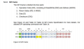
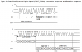
This example works interesting. The Master sends to the device and the slave doesn't send a dummy byte but a Status low byte and later a high byte (or maybe that's the dummy ;D). It works differently. So here if I want to send and receive data I have to use SPI_Transmit_Receive I guess ;> Because If I use SPI_Transmit then it ignores what it receives and is I use SPI_Receive then it ignores what it send to slave. And I guess TransmitReceive is transmiting 1 byte and receives 1 byte and reads both at the same time. It would work here watching the 10.2.1 I guess.

My example from first post works also differently but I think I slowly graps the idea. Because if I set to a multiple data receive then master sends one byte of data and the master only receives multiple bytes which means that master sends the dummy data (because first byte was with an autoincement bit for the device in the slave) so master doesn't send anything new.
 

Thread Starter

Xenon02

Joined Feb 24, 2021
504
3) Dummy data means just that. It can be any value. There is no such thing as manual vs automatic transmission.

4) The action taken depends on the meaning of the 8 bits received. This is application specific. You cannot apply the same meaning to all SPI applications.
Did I say partly correct in my post nr.35 ?
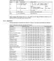
I did say something about "3)", That I understood that dummy byte can be anything, so I said what is what from an example and tried to explain why I said automatic and manual. I just read that maybe some devices requires to send a 0x00 which I heard it is a dummy byte ? or maybe it is never required ?

Like here :
1699040751803.png
Or here :

1699040767855.png

Sending some random bytes ?

Which I thought from the example nr.27 that when Master was reading, it sends 0x00 so I thought ok this is a dummy byte ? Does it count ? Then Why instead of reading I have to send something like dummy byte the device does it for itself like in the example nr.27 which turned the data from 11111111 into 00000000 and sends it to slave.


Did I somehow understood it in post nr. 37 ?
That If I want to read and write at the same time like in the diagram I have to use TrasmitReceive ? Because Transmit and Receive will make a gap. What I mean is Transmit will send data and the received data to master is ignored so the info is lost and Receive will read the byte the master receives but send dummy byte to slave which doesn't have to be the data it is said in the diagram.
 

Thread Starter

Xenon02

Joined Feb 24, 2021
504
I would like to leave the topic about dummy bytes, because I think I somehow managed to understand it partly (that it is specifiec in device).

Can someone although say if I am correct here or not ? :
I've seen a video that the SPI registers can have 16 bits like in STM32Nucleo, and they work in 8 bit format. The simple explanation of SPI is usually shown when registers have 8 bits and not 16 bits but also works in 8 bit format.

- Is it also device dependant how the SPI with 16 bit registers interprets its data ? It works in 8 bit format so my 1st proposition to how it could work is that first 8 bits are for transfer only and next 8 bits of the registeris for receive only and that's how it works for 8 bit format. Not a bad conclusion?

- If the SPI with 16 bit register works as 16 bit format and not 8 bit format, means that is must send 16 bits and receive 16 bit ? If so then Slave register must also have 16 bit to work in 16 bit format. That's what I thought of.

- If SPI works in 16 bit format then if Slave is in 8 bit format (want to receive 1 byte or 3 byte) it wouldn't work. So Slave must be also in 16 bit format.

- The size of registers can tell how maximally can be the format of SPI.

Please if it's possible tell in every point if they are okey/partly ok or completelly wrong. I want to know what I am standing on.
 

nsaspook

Joined Aug 27, 2009
16,426
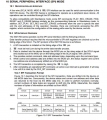
SPI technically be be any size (SPI allows word sizes of several bits, not necessarily rounded up to a multiple of 8, I've seen and used devices with odd-ball bits) but usually it's from 8 to 32-bits physical for each shift register. Most 32-bit processors allow for physical register byte sizes up to 32-bit to optimize transfers.
https://ww1.microchip.com/downloads/en/DeviceDoc/61106G.pdf

1699477356023.png

A 32-bit slave device.
https://www.mouser.com/catalog/specsheets/Murata_datasheet_sca3300_d01.pdf

1699477547606.png
It's basically about the device select frame size in bits between CS/SS device select toggles.
 
Top