The underlying point of "gate" design is the assumptions that gates have standard input and output levels. That "AND" gate's
output levels doesn't match the input levels your NOR gates depend on. The output needs to be close to ground for
a low input and close to Vcc for a high. The 2 1K resisters in series (assume an unreal 0 volt drop across both transistors)
leaves the output about 1/2 Vcc.
This is "logic gate design", not "logic gate use".
I'm not sure how much understanding you have of ohms law and transistors. Can you measure the voltages
on your circuit? You might learn a lot by measuring the voltage at the gate outputs and inputs (and transistor base voltages).
More on historical logic gate families: (Your NOR is a version of RTL resistor transistor logic)
Electronic is just my hobby, the next year i will go to univeristy for electical engereering I am also not engilsh so i have trouble learning on my own, but i will check theese links.
Its almost working but all the current is going to the inverter instead of my AND gate.
I deleted the unnecessary resistors so the voltage is near Vcc and Gnd.
I am atatching the txt inport file if you wannt to check it yourself, you can inport it in File -> inport from text
(https://www.falstad.com/circuit/circuitjs.html)
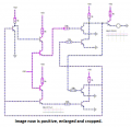
Why is your schematic a negative image with its parts so far apart that the parts and the text are tiny?
Please do it like this but without the Falstad dots:
Why is your schematic a negative image with its parts so far apart that the parts and the text are tiny?
Please do it like this but without the Falstad dots:
It seems to me that you're using a lot of transistors when something like this would work:
Can't remember if I ever breadboarded the circuit because I decided to go with R#S# because it simplified the counter logic, and I used BC547. I used the simulator between my ears to convince myself that it would work...
 Facebook
 Google
 GitHub
 Linkedin

") I am also not engilsh so i have trouble learning on my own, but i will check theese links.
I am also not engilsh so i have trouble learning on my own, but i will check theese links.