Facebook
 Google
 GitHub
 Linkedin
Hi,
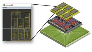
I am designing a standard 240 pin DDR3 UDIMM ram stick (16 DRAM chips, each 256M x 8 organisation, configured in dual rank configuration) for learning purposes. I did quite a lot of research on the DDR3 architecture and PCB layout, but there are still some questions that I can not answer on my own.
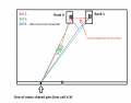
I know that on double-sided PCBs, it's preferred to have a via that connects the same pin on both (different rank) chips. But if you take it as a given, that you have two DRAM chips on the single side next to each other, what is the preferred routing style: fly by or T-branch?
1. If the T branch is preferred, should I split the track right at the beginning of the UDIMM module, or should I split it right before the minimum inevitable track length that is required to match the time skew for both chips?
2. If a fly by topology is preferred, is there any (approximate, experimental) maximum tolerable stub length with respect to the first daisy-chained chip?
I add a little sketch for clarification. Thank you in advance.
I am designing a standard 240 pin DDR3 UDIMM ram stick (16 DRAM chips, each 256M x 8 organisation, configured in dual rank configuration) for learning purposes. I did quite a lot of research on the DDR3 architecture and PCB layout, but there are still some questions that I can not answer on my own.
I know that on double-sided PCBs, it's preferred to have a via that connects the same pin on both (different rank) chips. But if you take it as a given, that you have two DRAM chips on the single side next to each other, what is the preferred routing style: fly by or T-branch?
1. If the T branch is preferred, should I split the track right at the beginning of the UDIMM module, or should I split it right before the minimum inevitable track length that is required to match the time skew for both chips?
2. If a fly by topology is preferred, is there any (approximate, experimental) maximum tolerable stub length with respect to the first daisy-chained chip?
I add a little sketch for clarification. Thank you in advance.
Attachments
-
 32.2 KB Views: 3