waveform generator

Thread Starter

robp1956

Joined Jun 12, 2026
107
I was using my waveform generator one morning tracing a signal through an amplifier. Then as I was tracing the signal it just disappeared nothing out from the waveform generator. I should note that it's a cheap one. I finally got it going again in a manner anyway. What I get out now from the output is a sine wave when every cycle starts I get a flat output for the first 1/2 of the positive going part the rest is as normal. Here is my problem I have the unit apart and every single chip used in the device has been laser etched off so there is no way to say what exactly to replace anything with even if I could find the problem chip. So to me and if someone brought it to me I would not fix it or even try to fix it. But this is mine and the only one I have so my instincts tell me that it is now E-waste but something will not let me send it to it's grave. Any advice as to where I should turn or are my instincts correct and it should be thrown out.
 

Thread Starter

robp1956

Joined Jun 12, 2026
107
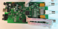
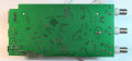
Supply voltage is 5V. but It looks like there is a boost converter on the board. I have pictures of the part of the board that I believe is a boost converter. I will post what Pictures I do have. Just the simple fact that there is not one thing on any chip that has not been laser etched off. even the transistors and MOSFETS not a number on any of them. including the 2 that are under the heatsink in the pictures.
 

Attachments

dl324

Joined Mar 30, 2015
18,418
I finally got it going again in a manner anyway.
What did you do to get to that point?
What I get out now from the output is a sine wave when every cycle starts I get a flat output for the first 1/2 of the positive going part the rest is as normal.
A scope picture would be helpful.
Here is my problem I have the unit apart and every single chip used in the device has been laser etched off so there is no way to say what exactly to replace anything with even if I could find the problem chip.
You can try tracing the circuitry back from the output and making a partial schematic. You can guess at the functionality of the 3 and 4 terminal devices based on how they're connected.

I troubleshot a B&K501A curve tracer that wasn't working. I didn't even have an oscilloscope at the time and did troubleshooting using a DVM and a logic probe. Traced the problem to an OR gate. Verified the fix after getting my first scope. Didn't acquire the manual until after that. The schematic wasn't included; I obtained that later.
 

Thread Starter

robp1956

Joined Jun 12, 2026
107
I do have a scope and I did try to trace the signal back and then forward from the CPU where the wave was perfect I lose it it seems at the Channel 1 output. there under the heat sink in the pictures. under that heat sink it looks like there are 4 MOSFETS in 2 6 pin packages one of those seems to be the offending chip. but again they are laser etched off so no clue as to what to replace them with. It looks like the waveform is output by those 4 MOSFETS. and of course they are smd chips. my nemesis. Now as for the scope trace I simply can't seem to get my scope to save a waveform to anything and I did try I even tried to get a photo of my screen but that looked terrible and not worth putting up here. If I can get my scope to save a screen I will post it here. I was in the process of figuring out what I wanted and what I was willing to pay for a new one as I knew that this one would not be as reliable as other equipment I have. I also figured it would have a limited useful lifetime. But that would be several months down the road. Now it seems it has to happen much sooner.
 

panic mode

Joined Oct 10, 2011
5,101
unfortunately those photos show nothing useful. all they do is give a tunnel vision...
since this is technical discussion and not nature photo contest, images need to be not just high quality but also easy to process (flip, mirror, line up one over another) to figure out circuit details that laser did not erase.

so how about nice, quality photos of both top AND bottom side of the PCB, covering full board and making sure that board orientation is actually parallel with the image edges? of course one can spend time and effort to manipulate photos and them them to suitable form but... why bother? i sure don't have much time to throw away. if you need help with this, help us see it better.
 

panic mode

Joined Oct 10, 2011
5,101
Ask and ye shall receive.
i think you misunderstood what was meant by top and bottom of the PCB. it means solder side and component side, all of the images show top side only, and no underside. can you post a link to documentation or place when this can be bought? need to see it inside and out.
 

Thread Starter

robp1956

Joined Jun 12, 2026
107
i think you misunderstood what was meant by top and bottom of the PCB. it means solder side and component side, all of the images show top side only, and no underside. can you post a link to documentation or place when this can be bought? need to see it inside and out.
Not sure what it's going to tell you. but here is the best your going to get short of you having the board in your hands. It's a somechineseguy design and somechineseguy does not publish a schematic to do that would negate having to laser etch every component.
 

Attachments

Thread Starter

robp1956

Joined Jun 12, 2026
107
That would be the one the 5206 claims 6MHZ but I found it to be not much better than 1 to 2 reliably. A very cheap signal generator and all I could afford at the time. Now looking into a new one this one was also very noisy down at 0.4V peak voltage so close to 1 volt peak to peak almost to noisy to get a trigger on it.
 

panic mode

Joined Oct 10, 2011
5,101
Not sure what it's going to tell you. but here is the best your going to get short of you having the board in your hands.
...
It's a somechineseguy design and somechineseguy does not publish a schematic to do that would negate having to laser etch every component.
it tells me that you cannot communicate well and that it takes effort to extract info out of you. people answering questions here are volunteering their time.
it would be really nice if those asking for help would attempt to not waste it.

not only you failed to reveal product name, model, external appearance etc. (cannot use reverse image lookup),
but your own images are very poor.

this is a technical forum. it would appreciated to show things in proper (technical) form.
2D/3D views need to be square and show normal (perpendicular/square) view, not slanted or trapezoid images.
They should be sharp/focused and subject shall occupy most of the image.

Showing clear front/back view is specially important if trying to determine function of components (chips not marked) because
following connections of top and bottom copper layers may be the only option left... and any squeue of the images (even slight)
makes it harder to match front and back of the solder pads and vias.

Not consider post by Danko, it shares external view of the product to identify it, along with two images of the board itself that are - square.

your idea of identifying it was "somechineseguy", no external view. and your images are in wrong form, out of focus etc.
some of your pictures have larger percentage of the image area dedicated to your own crotch than to board you need help with.

1783952160603.png

so why is this board not in portrait orientation, square and taking most of the visible space? why are parts of the board cleped even though 2/3 of image is wasted space?
if image did not come out perfect, use image editing tools to rotate, crop etc.

1783953042040.png
 

panic mode

Joined Oct 10, 2011
5,101
since the problem started suddenly, checking power section is one of first things to look at.
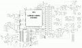
but looking at the schematics of the power section, i notice wrong D2 orientation.
 
I was using my waveform generator one morning tracing a signal through an amplifier. Then as I was tracing the signal it just disappeared nothing out from the waveform generator. I should note that it's a cheap one. I finally got it going again in a manner anyway. What I get out now from the output is a sine wave when every cycle starts I get a flat output for the first 1/2 of the positive going part the rest is as normal. Here is my problem I have the unit apart and every single chip used in the device has been laser etched off so there is no way to say what exactly to replace anything with even if I could find the problem chip. So to me and if someone brought it to me I would not fix it or even try to fix it. But this is mine and the only one I have so my instincts tell me that it is now E-waste but something will not let me send it to it's grave. Any advice as to where I should turn or are my instincts correct and it should be thrown out.
I wouldn’t throw it away yet. Since it is still producing a waveform, there is likely a fault in the output section rather than a complete failure. The flat area on the sine wave could be caused by clipping, a bad amplifier stage, or a power supply issue.

I would check the power rails, look for damaged components, and trace where the signal starts to fail. Even without chip markings, you may still be able to narrow down the problem. It may not be worth repairing commercially, but it could be a useful troubleshooting project.
 

Thread Starter

robp1956

Joined Jun 12, 2026
107
Wow I looked everywhere I could think of and never found this. Seems like my troubles from what I have been able to trace are in the output of channel 1 also feeds channel 2 through the relay. the 2 chips I thought were Mosfets it seems are transistors. they could be the problem or something behind it. Power seemed fine when I looked last so it's probably not anything on the power rail. Maybe I'll piece it together and give it another go. but this will help a lot. Thank you for that.
 

MrChips

Joined Oct 2, 2009
34,964
Wow I looked everywhere I could think of and never found this. Seems like my troubles from what I have been able to trace are in the output of channel 1 also feeds channel 2 through the relay. the 2 chips I thought were Mosfets it seems are transistors. they could be the problem or something behind it. Power seemed fine when I looked last so it's probably not anything on the power rail. Maybe I'll piece it together and give it another go. but this will help a lot. Thank you for that.
All I did was a Google image search for MHS-5200A schematics.

The first thing you should have stated upfront would have been the make and model. A picture of the front panel would have been useful. There is a lot of discussion of the MHS-5200A on Hackaday and EEVblog.
Hopefully there is a lesson learned here. Credit goes to Danko for identifying the unit.

Note that this is not an ordinary function generator. It is an AWG, arbitrary waveform generator. Some folks would give an arm and a leg to get their hands on one, including me. It is definitely worth fixing. Someone has reworked the User Manual in English. There is also info on communicating with a PC.
 

Thread Starter

robp1956

Joined Jun 12, 2026
107
I wouldn’t throw it away yet. Since it is still producing a waveform, there is likely a fault in the output section rather than a complete failure. The flat area on the sine wave could be caused by clipping, a bad amplifier stage, or a power supply issue.

I would check the power rails, look for damaged components, and trace where the signal starts to fail. Even without chip markings, you may still be able to narrow down the problem. It may not be worth repairing commercially, but it could be a useful troubleshooting project.
Yea and I did that but now I have a schematic I at least have an idea where things are and some idea of their place and use in the circuit. And I see what I thought was a boost converter actually is a boost converter generating + and - 13V. Not sure where that goes but the output only does 2V peak out. I suppose it could go to that ladder network for ADC conversion I assume. Just starting to figure out this CPU stuff I am going to need it if I plan on building a power supply.
 
Top