wanted short circuit Protection for LM338(TO-3)

panic mode

Joined Oct 10, 2011
5,178
not sure if it was stated but... what is the reason to use linear regulator for something that should handle large current and large voltage range? SMPS is simpler, cheaper, smaller etc. and no need for any heatsinks. and if you are one a shoe string budget, looking for PSU to power your projects, why not repurpose an old PC PSU? the old PCs are literally tossed away.
 

Thread Starter

ommsiva

Joined Mar 13, 2024
52
not sure if it was stated but... what is the reason to use linear regulator for something that should handle large current and large voltage range? SMPS is simpler, cheaper, smaller etc. and no need for any heatsinks. and if you are one a shoe string budget, looking for PSU to power your projects, why not repurpose an old PC PSU? the old PCs are literally tossed away.
Sir,

True, The Specification were truly involving large differential voltage when output voltage is small, which causes heat dissipation with linear regulators.

From where this spec came in my mind , i don't know. it always make me to think which is practically not achievable.

yes surely i am going through tl494 pwm based buck converter design where pulse width shall control the output voltage.

thank you.
 

ericgibbs

Joined Jan 29, 2010
21,535
hi omm,
I would also suggest a PWM PSU method.

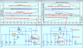
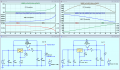
Just for reference only, a linear regulator using a high power bypass transistor and suitable heat sink can be used for high current linear regulators.
A simple example of their performance.

E

EG 1710.png
 

Thread Starter

ommsiva

Joined Mar 13, 2024
52
hi omm,
I would also suggest a PWM PSU method.

Just for reference only, a linear regulator using a high power bypass transistor and suitable heat sink can be used for high current linear regulators.
A simple example of their performance.

E

View attachment 355291
Sir,

1)Can please explain what is effective load connected to the circuit. how it is simulated?
from the third graph it says that resistance was increased from lower resistance (where current is higher) to higher resistance.

2) the second graph from bottom is power dissipation of regulator. but i cand understand the expression present at the top it
pd=(vin-vout)* Iload for voltage regulator

3) the third graph from bottom shows power dissipation of power transistor. But here also the expression present on top i cant understand?

pd=Vce * Iload=(vin-vload) * ILoad( here current larger than 75mA will be delivered by Power transistor)

kindly make me to understand these two expression and load resistance simulation.
 

ericgibbs

Joined Jan 29, 2010
21,535
hi omm,
You are misreading the text.

I have added more text details, it should help you understand the plots

The >> means changing.
E
EG 1710.png
 

bertus

Joined Apr 5, 2008
22,991
Hello,

@ericgibbs , how is the output voltage stability on your circuits?
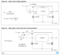
The booster circuits I have seen use a PNP transistor:
LM78XX_high_current.png
The circuits show a LM78XX, but it will likely also work with the LM317.

Bertus
 

drjohsmith

Joined Dec 13, 2021
1,631
Sir,

True, The Specification were truly involving large differential voltage when output voltage is small, which causes heat dissipation with linear regulators.

From where this spec came in my mind , i don't know. it always make me to think which is practically not achievable.

yes surely i am going through tl494 pwm based buck converter design where pulse width shall control the output voltage.

thank you.
wow ,
this post is going every where .

your now looking at a dcdc controler circuit,
that would certainly take care of the excess dissipation you were suffering, but has a complete new set of complications.

have you considered just using an off the shelf psu?
how much are you charging your time at ?
how much are you allowing for the pcb cost ?
 

ericgibbs

Joined Jan 29, 2010
21,535
@bertus,
In the past, using this version with 2N305X series they have worked well as 12V Lead Acid Battery chargers, powered by 24Vdc

I would be interested in running any particular stability test you would like me to investigate

E
 

drjohsmith

Joined Dec 13, 2021
1,631
fyi.
many people already have a cheap and ready supply of dc,
the standard pc power supply is often used in a lab environment
there are also online circuits / boards to allow a standard PC supply to be more user friendly terminals.
 

bertus

Joined Apr 5, 2008
22,991
Hello,

@ericgibbs , In your circuit with the NPN transistor , the output voltage will vary a bit with the drawn current , due to the chnge in the Vbe voltage.
In the PNP version that will not happen , as the Vbe is at the input of the regulator.

Bertus
 

ericgibbs

Joined Jan 29, 2010
21,535
@bertus,
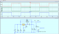
As the LM317 is also supplying current into the Load via the R3 resistor, the voltage across R3 (Vbe) will increase or decrease depending upon the load current. [ plot #3]

This sim plot shows, as an example, 14Vout [ as typical for a 12V SLA battery charger]

I have switched the load to show a load current between ~0.4A and 4.8A, the Vout changes ~188mV between these current values.

I would still recommend that the TS considers a more efficient SMPS unit.

E

EG 1713.png
 

drjohsmith

Joined Dec 13, 2021
1,631
@ericgibbs
always impressed how you guys can "knock up" a ltspice just like magic . I must find some time to learn .

your circuit is the sort of topology I'd expect for a current boosted lm317 , should there not be a diode across r2 though as part of the anti back power along with d1. should d1 not be a schotkey?

was also wondering, the op seems to want a ldo, no matter what,
and they seem to be able to blow up a hardened chip likevthe lm338,

should we be considering a psu with overcurrent shutdown, and some thermal limit ?

no guarantee the op won't find some reason again that the solution is not right , but ..
 

Thread Starter

ommsiva

Joined Mar 13, 2024
52
@ericgibbs
always impressed how you guys can "knock up" a ltspice just like magic . I must find some time to learn .

your circuit is the sort of topology I'd expect for a current boosted lm317 , should there not be a diode across r2 though as part of the anti back power along with d1. should d1 not be a schotkey?

was also wondering, the op seems to want a ldo, no matter what,
and they seem to be able to blow up a hardened chip likevthe lm338,

should we be considering a psu with overcurrent shutdown, and some thermal limit ?

no guarantee the op won't find some reason again that the solution is not right , but ..
Sir,
Definitely i will work with LM338 what i have , if it fails i will more curent boosting with LM317.

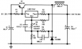
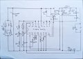
Here is a schematic with TL494 , i was working for past one week.
1757000523192.jpeg

TL494 Based Buck Converter – 0–30 V, 0–10 A (CC–CV)
1. Oscillator Design
• The buck converter operates at a switching frequency of 50 kHz.
• TL494 oscillator frequency is set by R9 and C2, using the formula:
F=1/R9C2
With R9=100K and C2=200pF
F=1/100K*200pF=50Khz
2. Voltage Control Loop
The voltage reference input for the error amplifier (inverting pin) varies between 0.42 V to 4.5 V, generated by:
• A 10 kΩ potentiometer,
• Divider network R1, R2, R3 (total 12 kΩ),
• 5 V reference from TL494.
• I=Vref/12K=5/12K=0.41mA taken by voltage divider network
• Voltage across lower end of 10K=0.41mA*1K=0.41V
• Voltage across Upper end of 10K=0.41mA*11K=4.5V
• It is non inverting amplifier where non inverting pin has voltage divider network (R12, R13) obtained from 5.6K and 1K. the output voltage of amplifier
• Vout =Vref (1+5.6K/1K); when voltage is taken from upper end of 10K
• Vout =4.5(1+5.6)
• Vout =29.7V
3. Current Control Loop
The current reference input varies from 10 mV to 100 mV, generated by:
• 10 kΩ potentiometer and divider network (R4, R5, R6) totalling 50 kΩ,
• 5 V reference from TL494.
• I =Vref/50K=5/50K=0.1mA taken by voltage divider network
• Voltage across lower end of 10K=0.1mA *100=10mV
• Voltage across Upper end of 10K=0.1mA *10100=110mV
• It is non inverting amplifier where non inverting pin has voltage developed across R14= 0.01Ω. when 10A current flows through the circuit, the voltage developed across the circuit will be 100mV.
When the sensed voltage exceeds the set reference, the PWM duty cycle is reduced, thereby limiting the output current.
4. TL494 Output Stage
• Output transistors of TL494 are used in common-emitter configuration.
o Pins 9 & 10 (emitters) tied to ground.
o Pins 8 & 11 (collectors) connected together to drive the external transistor stage (Q1, Q2).
• Pin 13 (Output Control) tied to ground → enables single-ended mode (both outputs in phase).
5. Output Filter
• The LC output filter is designed using TI reference design guidelines (SLVS0741).
• Inductor (L) = 150 µH
• Output capacitor (C3) = 1000 µF / 63 V (low ESR)
• Freewheeling diode (D6) = fast recovery or Schottky type, rated ≥30 A, ≥60 V

6. Input Stage
• Input from a 24–0–24 V / 10 A transformer.
• Rectified peak voltage:
Vpeak=24*1.414=34V
• After rectifier drops and filtering: ≈32 V DC available.
• Input capacitor (C1) = 50,000 µF / 63 V electrolytic.
• Bridge rectifier made from 10A10 diodes.

Its a theoretical design. I have not Constructed yet.

Kindly correct the flaws present in the circuit.
 

drjohsmith

Joined Dec 13, 2021
1,631
Sir,
Definitely i will work with LM338 what i have , if it fails i will more curent boosting with LM317.

Here is a schematic with TL494 , i was working for past one week.
View attachment 355367

TL494 Based Buck Converter – 0–30 V, 0–10 A (CC–CV)
1. Oscillator Design
• The buck converter operates at a switching frequency of 50 kHz.
• TL494 oscillator frequency is set by R9 and C2, using the formula:
F=1/R9C2
With R9=100K and C2=200pF
F=1/100K*200pF=50Khz
2. Voltage Control Loop
The voltage reference input for the error amplifier (inverting pin) varies between 0.42 V to 4.5 V, generated by:
• A 10 kΩ potentiometer,
• Divider network R1, R2, R3 (total 12 kΩ),
• 5 V reference from TL494.
• I=Vref/12K=5/12K=0.41mA taken by voltage divider network
• Voltage across lower end of 10K=0.41mA*1K=0.41V
• Voltage across Upper end of 10K=0.41mA*11K=4.5V
• It is non inverting amplifier where non inverting pin has voltage divider network (R12, R13) obtained from 5.6K and 1K. the output voltage of amplifier
• Vout =Vref (1+5.6K/1K); when voltage is taken from upper end of 10K
• Vout =4.5(1+5.6)
• Vout =29.7V
3. Current Control Loop
The current reference input varies from 10 mV to 100 mV, generated by:
• 10 kΩ potentiometer and divider network (R4, R5, R6) totalling 50 kΩ,
• 5 V reference from TL494.
• I =Vref/50K=5/50K=0.1mA taken by voltage divider network
• Voltage across lower end of 10K=0.1mA *100=10mV
• Voltage across Upper end of 10K=0.1mA *10100=110mV
• It is non inverting amplifier where non inverting pin has voltage developed across R14= 0.01Ω. when 10A current flows through the circuit, the voltage developed across the circuit will be 100mV.
When the sensed voltage exceeds the set reference, the PWM duty cycle is reduced, thereby limiting the output current.
4. TL494 Output Stage
• Output transistors of TL494 are used in common-emitter configuration.
o Pins 9 & 10 (emitters) tied to ground.
o Pins 8 & 11 (collectors) connected together to drive the external transistor stage (Q1, Q2).
• Pin 13 (Output Control) tied to ground → enables single-ended mode (both outputs in phase).
5. Output Filter
• The LC output filter is designed using TI reference design guidelines (SLVS0741).
• Inductor (L) = 150 µH
• Output capacitor (C3) = 1000 µF / 63 V (low ESR)
• Freewheeling diode (D6) = fast recovery or Schottky type, rated ≥30 A, ≥60 V

6. Input Stage
• Input from a 24–0–24 V / 10 A transformer.
• Rectified peak voltage:
Vpeak=24*1.414=34V
• After rectifier drops and filtering: ≈32 V DC available.
• Input capacitor (C1) = 50,000 µF / 63 V electrolytic.
• Bridge rectifier made from 10A10 diodes.

Its a theoretical design. I have not Constructed yet.

Kindly correct the flaws present in the circuit.
the lm338 fails because you have either.
a. wired it in wrong
b. its a fake part
c. your just unlucky
d. you had reverse voltage it with big capacitance on output and disconnecting the input .

of these , b seems the most likely ,
why do you think that switching to a 317 which has much less protection than the 338 will be better ?

why after weeks of duscusion, and changing requirements, have you now "randomly" chosen yet another chip ?

designing you own smps , winding or finding the right inductor, and pcb layout are not to be undertaken lightly ,
 

Thread Starter

ommsiva

Joined Mar 13, 2024
52
the lm338 fails because you have either.
a. wired it in wrong
b. its a fake part
c. your just unlucky
d. you had reverse voltage it with big capacitance on output and disconnecting the input .

of these , b seems the most likely ,
why do you think that switching to a 317 which has much less protection than the 338 will be better ?

why after weeks of duscusion, and changing requirements, have you now "randomly" chosen yet another chip ?

designing you own smps , winding or finding the right inductor, and pcb layout are not to be undertaken lightly ,
Sir ,

Long back I started nearly 4 years . Starting with 1amps, then 3amp all were working and with lm317 and lm350 with out any external circuit added to it.


Now 2 years back i started with 5amp. All these experience were derived by failing n number of time because it's my circuit has to control 150watt of power.

All by explanation , calculation will show my understanding.

All your replies portrays that I am wasting All your time. Not at all.


Thank you all.
 
Top