UJT transistor simple operating principle?

Thread Starter

Saviour Muscat

Joined Sep 19, 2014
187
Hello guys,

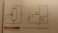
Please refer to the figure attached,
My query is: the basic operating principle of UJT transistor, I understood as follows:
Suppose the emitter supply is turned down to zero, The voltage(potential divider or intrinsic stand off voltage) between the two internal resistance UJT reverse biases the emitter diode . When you bring up the emitter supply until its slightly larger than the voltage of the potential divider , the lower internal resistor of the UJT drops its resistance significantly and the emitter diode conducts and large current passes from the emitter diode to the lower internal resistor(dropped in value) to ground.
Please can someone corrects or confirm my thoughts ?
Thanks
Saviour Muscat
 

Attachments

Thread Starter

Saviour Muscat

Joined Sep 19, 2014
187
Thanks for your reply
I think the link you provided is not too much explained but I think negative resistance is explained as I quoted Please correct me if am I wrong.
When you bring up the emitter supply until its slightly larger than the voltage of the potential divider , the lower internal resistor of the UJT drops its resistance significantly and the emitter diode conducts and large current passes from the emitter diode to the lower internal resistor(dropped in value) to ground.
 

Thread Starter

Saviour Muscat

Joined Sep 19, 2014
187
I try
Please refer to the link http://hyperphysics.phy-astr.gsu.edu/hbase/electronic/relaxo.html#c1
1 When CT charges, Vout increases( firstly the emitter diode is open), until the voltage across the capacitor is slightly bigger than intrinsic stand off voltage of UJT(emitter diodes conduct), therefore the capacitor discharges through emitter diode and through to decreased resistance of the lower base resistor and through R1 ,finally vout drops to zero and repeat it self
 
Last edited:

studiot

Joined Nov 9, 2007
4,998
My query is: the basic operating principle of UJT transistor, I understood as follows:
Suppose the emitter supply is turned down to zero, The voltage(potential divider or intrinsic stand off voltage) between the two internal resistance UJT reverse biases the emitter diode . When you bring up the emitter supply until its slightly larger than the voltage of the potential divider , the lower internal resistor of the UJT drops its resistance significantly and the emitter diode conducts and large current passes from the emitter diode to the lower internal resistor(dropped in value) to ground.
Ok your description is basically correct, but a few extra points.

Firstly the current is to negative, which may or may not be connected to ground.

I would add that the bar semiconductor between the bases represents an ohmic path of between 5k and 10 ohms.

So if we make the top connection positive and the bottom one negative, without connecting the emitter, a current flows in the bar of material between and the potential varies along the bar from +V at the top to -V (or zero) at the bottom. Say the top (base 2 or B") is at V2 and the bottom (base1 or B1) at 0 for simplicity.

So the emitter is at some intermediate voltage \(\eta V\) due to its location along the bar.

If we now apply an external bias < \(\eta V\), the PN emitter base junction will be reverse biased and only leakage current will flow through the emitter junction.

Similarly if we apply an external bias >\(\eta V\) the PN junction will be forward biased then a large emitter current will be i jected into the bar at this point.
This current consistes largely of hole current injected into bar moving towards B1 which draws a corresponding electron current into the section of bar between the emitter and B1.
These causes the conductivity of this section of bar to rise and the potential of the emitter to drop.
 
Top