Facebook
 Google
 GitHub
 Linkedin
Hi all,
I have a transistor which need to act as a switch.
This is my transistor : https://www.onsemi.com/pub/Collateral/MMBTA05LT1-D.PDF - MMBTA06
I need to make sure that this works in either saturation or cut off region only. It must not work the active region.
In order for the transistor to work in the active region, the Base emitter region should be forward biased and the base collector junction should be reverse biased.
So, if I donot maintain the above condition, the transistor would not enter in the active region, right?
Is there any graph there in the datasheet which is indicative of the maximum limits(Ic vs Vbe sat graph, of Vce vs gain graph etc..) to make sure that I don't enter the active region of the transistor? Please help me understand.


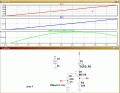
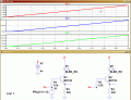
") The chart shows the collector voltage entering saturation as the collector voltage vs current becomes close to being asymptotic to the horizontal.
The chart shows the collector voltage entering saturation as the collector voltage vs current becomes close to being asymptotic to the horizontal.