Facebook
 Google
 GitHub
 Linkedin
Okay Eric.Hi D,
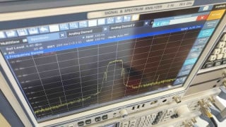
By bypassing the 768K resistor with the 1000pF the response to high going Vout spikes, it will increase the Vfb thus pull down the Vout faster to the desired Vout.
Personally, I would not include the 49.9R and 1nF
E
TPS61088 - Design and testing
- Thread starter Dikxita
- Start date