Facebook
 Google
 GitHub
 Linkedin
Hello AAC-Members,
I want to preface this by saying that I'm really new to PCB-Design.
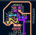
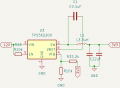
I have designed this fairly simple PCB with a Texas Instruments TPS562201DDCR step-down voltage regulator. It is supposed to step-down 12V to 3.3V for a microcontroller.
After soldering just the TPS related circuitry and testing it out, however, it blew. I tried on multiple boards with the TPS flipped. (Couldn't, and still can't, figure out where PIN 1 is on these chips, I assume it is where the bar is located, but that's besides the point)
Can someone point out to me what I'm doing wrong? I quintessentially copied and slightly modified the example circuit in the datasheet of the IC (Page 12).


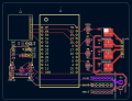
(Regarding the attached pictures; I disabled the back copper-layer for visual clarity, no footprint is placed there, only traces connecting Via's)
Thanks in advance and best regards
I want to preface this by saying that I'm really new to PCB-Design.
I have designed this fairly simple PCB with a Texas Instruments TPS562201DDCR step-down voltage regulator. It is supposed to step-down 12V to 3.3V for a microcontroller.
After soldering just the TPS related circuitry and testing it out, however, it blew. I tried on multiple boards with the TPS flipped. (Couldn't, and still can't, figure out where PIN 1 is on these chips, I assume it is where the bar is located, but that's besides the point)
Can someone point out to me what I'm doing wrong? I quintessentially copied and slightly modified the example circuit in the datasheet of the IC (Page 12).
(Regarding the attached pictures; I disabled the back copper-layer for visual clarity, no footprint is placed there, only traces connecting Via's)
Thanks in advance and best regards
Attachments
-
 137.8 KB Views: 4
 -
 302.2 KB Views: 4


")