Facebook
 Google
 GitHub
 Linkedin
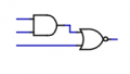
Yes, the function of the half-comparator is indeed rather unusual! (In retrospect it was a poor naming choice because that isn't what it does at all.) Basically it outputs HI if all of the pins are LO, if only one of the inputs is HI, or if both of the LSB inputs are HI. Otherwise it outputs a LO signal. And of course in operation two of its inputs will be inverted externally (which is probably why at a glance it appears that the bits in each position can be independently swapped without affecting the output). Within the 2-bit comparator the "upper stage" LX pins are inverted, likewise for the "lower stage" RX input pins.Correctness is the most important part -- it doesn't matter how fast, small, or cheap it is if it doesn't work.
It took me a while to figure out your approach and I thought I had done so, but after a closer inspection, I'm not sure. I would really help if you described the idea behind how your circuits work, a description of what the inputs and outputs mean, and truth tables of how they are intended to behave.
I'll try to walk though how my attempt to reverse engineer your circuit lead me to think and you can correct me where I've missed the mark.
My first impression was that your overall circuit is taking two 2-bit inputs, R and L, with the msb each being suffixed with H and the lsb suffixed with L. It is then producing two outputs, LG and RG, in which
LG = L>R?
RG = L<R?
With this supposition in mind, I then concluded (a conclusion that I am seriously questioning, however) that your half comparator answered the question
out = L>R (or L<R)
and that the idea was that you would swap L and R inputs to one of them to get the other, thus giving you both LT and GT outputs. But that doesn't seem to be what's happening since you aren't changing the L/R orientation, but instead taking the ones complement of one or the other. But perhaps this accomplishes the same thing.
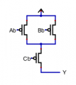
My next point of concern is that your half-comparator circuit seems to be symmetric regarding L and R, meaning that they can be swapped without affecting the output. More troubling is that it appears that the bits in each position can be independently swapped without affecting the output. Either of these would render it incapable to properly distinguishing between L and R values properly. But perhaps my visual inspection is missing something.
To see one instance of this, consider just the LL and RL inputs to the half-comparator. The only place these two inputs go are to a 2-input NOR gate and it doesn't matter which one goes to which since NOR is symmetric. Assuming that LL is the lsb of the left number and RL is the lsb of the right, this means that the circuit will produce the same output for L=00, R=01 as it does for L=01, R=00.
I'll try to explore this a bit deeper later.
Everything does seem to be working properly but I suspect that there could be some simplification done. I will work on it some more over the week. (Just let me know if you would like a link to simulation. I can wrap the whole circuit into a text file which can then be loaded by the Falstad simulator.)
Just out of curiosity, how few transistors do you think the 2-bit comparator could be implemented with? Right now the number needed to make an N-bit comparator with this design amounts to 60*(N-1) transistors. (Which means a 64-bit comparator would weigh in at 3780 MOSFETs!) That sure seems like a lot to me.
Last edited:


")