Facebook
 Google
 GitHub
 Linkedin
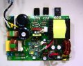
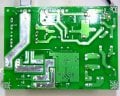
I am currently working on a Samlex SEC-1235 switch mode power supply and I have no DC voltage output. It should be in the area of 13.6 VDC. I am to the point that I believe I have a bad switching transistor. I have tested it like a bipolar but it does not make sense to me. Is there another way to test them? The two readings are different from each other which would confirm my suspicions but would like to know more about them.
Testing Switching Transistors
- Thread starter bwilliams60
- Start date