T Flip Flop

Thread Starter

PG1995

Joined Apr 15, 2011
832
Hi,

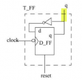
I was trying to understand the operation of a T Flip Flop. I have seen the diagram shown below in one of the books as well where input is applied at Q.

CE is an enable input and it is assumed that the flip flop is negative edge triggered.

Question:
If "1" is applied on Qn, the flip flop will produce 0 on Q(n+1). The same node Q is "1" and "0". Isn't it contradictory?

1649059469800.png
Source: https://www.cse.psu.edu/~kxc104/class/cmpen271/13f/hw/hw8/hw8.html

1649059735085.png
T flop flop truth table
 

Ian0

Joined Aug 7, 2020
9,817
That's not a great truth table.
Q is always an output, never an input.
Qn and Q(n+1) both refer to the same output, they are not contradictory, because Qn mean the present state of the output and Q(n+1) means the state of the SAME output but after the NEXT clock pulse.
Q(n-1) would refer the the state of the same output before the last clock pulse.
Your truth table should show a column for CLK, which should contain a ^ (up arrow) indicating a rising edge on the input.
So, what actually happens is that the Q output AFTER the clock pulse is equal to the D input BEFORE the clock pulse.
If D = not(Q) (the effect of the inverter) then every time there is a rising edge on CLK the output changes to the opposite state.
 

Thread Starter

PG1995

Joined Apr 15, 2011
832
Thank you, @ericgibbs

I understand the basic operation of T flip flip but the shown configuration in my previous messages confused me where an inverter is used with D flip flip to make a T flip flop/
 

Thread Starter

PG1995

Joined Apr 15, 2011
832
That's not a great truth table.
Q is always an output, never an input.
Qn and Q(n+1) both refer to the same output, they are not contradictory, because Qn mean the present state of the output and Q(n+1) means the state of the SAME output but after the NEXT clock pulse.
Q(n-1) would refer the the state of the same output before the last clock pulse.
Your truth table should show a column for CLK, which should contain a ^ (up arrow) indicating a rising edge on the input.
So, what actually happens is that the Q output AFTER the clock pulse is equal to the D input BEFORE the clock pulse.
If D = not(Q) (the effect of the inverter) then every time there is a rising edge on CLK the output changes to the opposite state.
I think I understand it now. The diagram shown below confused me. The part highlighted in yellow gave me the impression as if the Q is also the input, i.e. the input is applied at the highlighted part.

1649061043434.png
 

Delta Prime

Joined Nov 15, 2019
1,311
Hi,

I was trying to understand the operation of a T Flip Flop. I have seen the diagram shown below in one of the books as well where input is applied at Q.

CE is an enable input and it is assumed that the flip flop is negative edge triggered.

Question:
If "1" is applied on Qn, the flip flop will produce 0 on Q(n+1). The same node Q is "1" and "0". Isn't it contradictory?

View attachment 264226
Source: https://www.cse.psu.edu/~kxc104/class/cmpen271/13f/hw/hw8/hw8.html

View attachment 264227
T flop flop truth table
Your schematic shows a positive edge trigger here.1649063836716.png
I think I understand it now. The diagram shown below confused me. The part highlighted in yellow gave me the impression as if the Q is also the input, i.e. the input is applied at the highlighted part.

View attachment 264236
Your schematic shows a negative edge trigger here.1649063866495.png
As a supplement .
While the clock is going from 0 to 1
D is read & propagates almost immediately to output Q . The value of D at the positive edge for a positive edge trigger D flip flop matters . What you have is a negative edge trigger D flip flop indicated by the little bubble on the clock input. Keep in mind there will be a propagation delay as D is read
1649061922811.jpg
 

Papabravo

Joined Feb 24, 2006
21,225
A basic principle of logic circuits is that you never apply an input to an output pin. The output pin can be routed to other places which may not be shown in the diagram. The reason for showing the inverter is that some flip-flops do not have complementary outputs available. So, the Q-bar output must be generated with an inverter.
 

AnalogKid

Joined Aug 1, 2013
11,044
I think I understand it now. The diagram shown below confused me. The part highlighted in yellow gave me the impression as if the Q is also the input, i.e. the input is applied at the highlighted part.
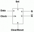
Correct. In digital logic schematic symbols, Q almost always designates an output, and D almost always is an input. BTW, the standard is to use capital letters. Also, it us very common for pins to be arranged such that inputs are on the left and outputs on the right. Of course there are exceptions. In the image below, S and R are inputs. For some unknown reason, it is common for flipflops to be drawn this way. Always check the datasheet.

Note that with real-world devices, there usually is a complimentary output (Q with a bar over it, -Q, Q-, Q*, *Q, etc.) available, and this output is connected directly to the D input so you do not need the inverter. Complimentary outputs have a bubble just like negative-true inputs. Here is the symbol for one-half of a CD4013, but it is missing the -Q bubble:

1649078341287.png

ak
 
Last edited:
Top