 Facebook
 Google
 GitHub
 Linkedin
Hello all, i was trying to build a circuit that uses LM2903B, which is a comparator, what i wanna obtain is a square wave with 50% dutycycle and frequency at 10KHz.
First of all i calculated the symmetry point at V+ pin, which has to be 50% of vcc, which is 2.5V, i chose to put 2 resistors of 51kOhm as voltage divider to do so, then i calculated the RH needed in order to have the hysteresis which creates a voltage divider beetwen Vref and Vout. we want to have that the capacitor charges from 1/3vcc to 2/3vcc and discharges from 2/3vcc to 1/3vcc, the vcc is 5V so we got VT+ = 3.33V and VT- = 1.67V
so V+ = Vref + ( VCC - Vref ) * Rdiv/RH+Rdiv, by putting the numbers and doing calculations i get that RH has to be 51kohm for 50% duty cycle
for the frequency i used this formula:
f = 1/2R5C*ln ( VCC-VT-/VCC-VT+) and by choosing the capacitor as 10nF i found R5=7.21kOhm
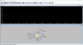
But i got an issue, when im making the simulation i dont see a square wave , but a d.c wave fixed at 2.5V? can u explain me? consider that im not that good so please try to explain in simple way thanks
First of all i calculated the symmetry point at V+ pin, which has to be 50% of vcc, which is 2.5V, i chose to put 2 resistors of 51kOhm as voltage divider to do so, then i calculated the RH needed in order to have the hysteresis which creates a voltage divider beetwen Vref and Vout. we want to have that the capacitor charges from 1/3vcc to 2/3vcc and discharges from 2/3vcc to 1/3vcc, the vcc is 5V so we got VT+ = 3.33V and VT- = 1.67V
so V+ = Vref + ( VCC - Vref ) * Rdiv/RH+Rdiv, by putting the numbers and doing calculations i get that RH has to be 51kohm for 50% duty cycle
for the frequency i used this formula:
f = 1/2R5C*ln ( VCC-VT-/VCC-VT+) and by choosing the capacitor as 10nF i found R5=7.21kOhm
But i got an issue, when im making the simulation i dont see a square wave , but a d.c wave fixed at 2.5V? can u explain me? consider that im not that good so please try to explain in simple way
thanksAttachments
-
 57 KB Views: 11
 -
1.6 KB Views: 4


