Facebook
 Google
 GitHub
 Linkedin
Hello,
I am developing the code for my PIC32MK1024MCM project. I have already tested the code well and now I am only putting all the code modules into the final project (the code is not complete in this example yet, but the functionality is not the axis of interest here). For the first time in my life, I wanted to make it a little bit more professional and use separate source and header files for all the different module function declaration. However, I am clearly facing some kind of syntax problem, because I am getting errors in almost every line of the source file (I guess I have to include something in that source file, but I am not sure) Like I said, it is my very first time facing header and source files, so could you please help me, or at least hint me, what is it that I am missing so obviously? I want to thank you in advance.
main:
configurations_bits
analog_to_digital_conversion.h
analog_to_digital_conversion.c
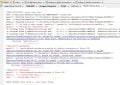
I also tried including "definitions.h" at the top of the source file, but still, I am getting errors (depicted in the pictures)
I am developing the code for my PIC32MK1024MCM project. I have already tested the code well and now I am only putting all the code modules into the final project (the code is not complete in this example yet, but the functionality is not the axis of interest here). For the first time in my life, I wanted to make it a little bit more professional and use separate source and header files for all the different module function declaration. However, I am clearly facing some kind of syntax problem, because I am getting errors in almost every line of the source file (I guess I have to include something in that source file, but I am not sure) Like I said, it is my very first time facing header and source files, so could you please help me, or at least hint me, what is it that I am missing so obviously? I want to thank you in advance.
main:
Code:
#include <xc.h>
#include <configuration_bits.c>

#include <toolchain_specifics.h>
#include <stddef.h>
#include <stdint.h>
#include <stdbool.h>
#include <stdlib.h>
#include "stdio.h"
#include <sys/attribs.h>

#include <analog_to_digital_conversion.h>

    void main(void) {


            while (1){

            }

        return (EXIT_FAILURE);

    }
Code:
// DEVCFG3
#pragma config USERID = 0xFFFF // Enter Hexadecimal value (Enter Hexadecimal value)
#pragma config PWMLOCK = OFF // PWM IOxCON lock (PWM IOxCON register writes accesses are not locked or protected)
#pragma config FUSBIDIO2 = OFF // USB2 USBID Selection (USBID pin is controlled by the port function)
#pragma config FVBUSIO2 = OFF // USB2 VBUSON Selection bit (VBUSON pin is controlled by the port function)
#pragma config PGL1WAY = OFF // Permission Group Lock One Way Configuration bit (Allow multiple reconfigurations)
#pragma config PMDL1WAY = OFF // Peripheral Module Disable Configuration (Allow multiple reconfigurations)
#pragma config IOL1WAY = OFF // Peripheral Pin Select Configuration (Allow multiple reconfigurations)
#pragma config FUSBIDIO1 = OFF // USB1 USBID Selection (USBID pin is controlled by the port function)
#pragma config FVBUSIO1 = OFF // USB2 VBUSON Selection bit (VBUSON pin is controlled by the port function)

// DEVCFG2
#pragma config FPLLIDIV = DIV_1 // System PLL Input Divider (1x Divider)
#pragma config FPLLRNG = RANGE_BYPASS // System PLL Input Range (Bypass)
#pragma config FPLLICLK = PLL_POSC // System PLL Input Clock Selection (POSC is input to the System PLL)
#pragma config FPLLMULT = MUL_4 // System PLL Multiplier (PLL Multiply by 4)
#pragma config FPLLODIV = DIV_2 // System PLL Output Clock Divider (2x Divider)
#pragma config BORSEL = HIGH // Brown-out trip voltage (BOR trip voltage 2.1v (Non-OPAMP deviced operation))
#pragma config UPLLEN = OFF // USB PLL Enable (USB PLL Disabled)

// DEVCFG1
#pragma config FNOSC = POSC // Oscillator Selection Bits (Primary Osc (HS,EC))
#pragma config DMTINTV = WIN_0 // DMT Count Window Interval (Window/Interval value is zero)
#pragma config FSOSCEN = OFF // Secondary Oscillator Enable (Disable Secondary Oscillator)
#pragma config IESO = ON // Internal/External Switch Over (Enabled)
#pragma config POSCMOD = HS // Primary Oscillator Configuration (HS osc mode)
#pragma config OSCIOFNC = OFF // CLKO Output Signal Active on the OSCO Pin (Disabled)
#pragma config FCKSM = CSDCMD // Clock Switching and Monitor Selection (Clock Switch Disabled, FSCM Disabled)
#pragma config WDTPS = PS1 // Watchdog Timer Postscaler (1:1)
#pragma config WDTSPGM = STOP // Watchdog Timer Stop During Flash Programming (WDT stops during Flash programming)
#pragma config WINDIS = NORMAL // Watchdog Timer Window Mode (Watchdog Timer is in non-Window mode)
#pragma config FWDTEN = OFF // Watchdog Timer Enable (WDT Disabled)
#pragma config FWDTWINSZ = WINSZ_25 // Watchdog Timer Window Size (Window size is 25%)
#pragma config DMTCNT = DMT31 // Deadman Timer Count Selection (2^31 (2147483648))
#pragma config FDMTEN = OFF // Deadman Timer Enable (Deadman Timer is disabled)

// DEVCFG0
#pragma config DEBUG = OFF // Background Debugger Enable (Debugger is disabled)
#pragma config JTAGEN = OFF // JTAG Enable (JTAG Disabled)
#pragma config ICESEL = ICS_PGx1 // ICE/ICD Comm Channel Select (Communicate on PGEC1/PGED1)
#pragma config TRCEN = OFF // Trace Enable (Trace features in the CPU are disabled)
#pragma config BOOTISA = MIPS32 // Boot ISA Selection (Boot code and Exception code is MIPS32)
#pragma config FECCCON = ECC_DECC_DISABLE_ECCON_WRITABLE // Dynamic Flash ECC Configuration Bits (ECC and Dynamic ECC are disabled (ECCCON<1:0> bits are writable))
#pragma config FSLEEP = OFF // Flash Sleep Mode (Flash is powered down when the device is in Sleep mode)
#pragma config DBGPER = PG_ALL // Debug Mode CPU Access Permission (Allow CPU access to all permission regions)
#pragma config SMCLR = MCLR_NORM // Soft Master Clear Enable (MCLR pin generates a normal system Reset)
#pragma config SOSCGAIN = G3 // Secondary Oscillator Gain Control bits (Gain is G3)
#pragma config SOSCBOOST = ON // Secondary Oscillator Boost Kick Start Enable bit (Boost the kick start of the oscillator)
#pragma config POSCGAIN = G3 // Primary Oscillator Coarse Gain Control bits (Gain Level 3 (highest))
#pragma config POSCBOOST = ON // Primary Oscillator Boost Kick Start Enable bit (Boost the kick start of the oscillator)
#pragma config POSCFGAIN = G3 // Primary Oscillator Fine Gain Control bits (Gain is G3)
#pragma config POSCAGCDLY = AGCRNG_x_25ms // AGC Gain Search Step Settling Time Control (Settling time = 25ms x AGCRNG)
#pragma config POSCAGCRNG = ONE_X // AGC Lock Range bit (Range 1x)
#pragma config POSCAGC = Automatic // Primary Oscillator Gain Control bit (Automatic Gain Control for Oscillator)
#pragma config EJTAGBEN = NORMAL // EJTAG Boot Enable (Normal EJTAG functionality)

// DEVCP
#pragma config CP = OFF // Code Protect (Protection Disabled)

// SEQ
#pragma config TSEQ = 0xFFFF // Boot Flash True Sequence Number (Enter Hexadecimal value)
#pragma config CSEQ = 0xFFFF // Boot Flash Complement Sequence Number (Enter Hexadecimal value)
Code:
//**************************************************************************
// ANALOG TO DIGITAL CONVERSION HEADER FILE
//**************************************************************************

  #include <analog_to_digital_conversion.c>

    void Anaolog_to_Digital_Conversion_Setup (void);

    void Anaolog_to_Digital_Conversion_Enable (void);

    void Anaolog_to_Digital_Conversion_Disable (void);

    uint16_t Anaolog_to_Digital_Conversion (void);
Code:
//**************************************************************************
// ANALOG TO DIGITAL CONVERSION SOURCE FILE
//**************************************************************************

    void Anaolog_to_Digital_Conversion_Setup (void){

        //All this procedure is taken from the device`s datasheet (no ADC interrupts are desired)

        ADCANCONbits.ANEN5 = 0b0; //Analog and bias circuitry disabled (to set calibration)
        //---------------------------------------------------------------------------------------------------------------------------------------------------------------
        ADC5CFGbits.ADCCFG = DEVADC5; //Copying the factory calibration ADC module bits to the ADC configuration register
        //---------------------------------------------------------------------------------------------------------------------------------------------------------------
        ADCCON1bits.ON = 0b0; //Disabling the ADC module
        //---------------------------------------------------------------------------------------------------------------------------------------------------------------
        ADC5TIMEbits.SAMC = 0b1111111111; //Sample time is set to 1025 TAD
        ADC5TIMEbits.ADCDIV = 0b1111111; //254 * TQ = TAD (ADC clock division bits)
        //---------------------------------------------------------------------------------------------------------------------------------------------------------------
        ADCANCONbits.WKUPCLKCNT = 0xF; //ADC warm up time is set to 32768 ADC clock cycles (maximum warm up time, around 32 us @ 100 MHz SYSCLK)
        //---------------------------------------------------------------------------------------------------------------------------------------------------------------
        ADCCON3bits.ADCSEL = 0b0; //Analog-to-Digital Clock Source (TCLK) -> SYSCLK
        ADCCON3bits.CONCLKDIV = 0b000000; //TCLK = TQ
        ADCCON3bits.DIGEN5 = 0b0; //All digital bits are disabled (according to the datasheet)
        ADCCON3bits.VREFSEL = 0b000; //Vref is set to AVdd and AVss
        //---------------------------------------------------------------------------------------------------------------------------------------------------------------
        ADCIMCON1bits.DIFF11 = 0b0; //AN11 is using Single-ended mode
        ADCIMCON1bits.SIGN11 = 0b0; //AN11 is using Unsigned Data mode
        //---------------------------------------------------------------------------------------------------------------------------------------------------------------
        ADCTRGSNSbits.LVL11 = 0b0; //Analog input is sensitive to the positive edge of its trigger (this is the value after a reset)
        //---------------------------------------------------------------
        ADCTRG3bits.TRGSRC11 = 0b00001; //AN11 is software triggered
        //---------------------------------------------------------------------------------------------------------------------------------------------------------------
        ADCANCONbits.ANEN5 = 0b1; //Analog and bias circuitry enabled
        //---------------------------------------------------------------------------------------------------------------------------------------------------------------
        ADCCON1bits.ON = 0b1; //Enabling the ADC module
        //---------------------------------------------------------------
        while(!((ADCCON2bits.BGVRRDY)&&(ADCANCONbits.WKRDY5))); //Wait until device analog environment is ready
        ADCCON3bits.DIGEN5 = 0b1; //Enable digital circuitry for data processing
        //---------------------------------------------------------------------------------------------------------------------------------------------------------------
        ADCCON3bits.ADINSEL = 0b001011; //Select analog channel 11 for conversion
        //---------------------------------------------------------------------------------------------------------------------------------------------------------------
        ADCCON1bits.ON = 0b0; //Disabling the ADC module
}Attachments
-
 184 KB Views: 3
 -
 197.5 KB Views: 3