Soldering and heat damage

Thread Starter

infy

Joined Jun 18, 2020
13
Hey everyone - my first post here since I realized I could use some advice. To set some context.. I'm a hobbyist just trying to get a simple circuit together. But I've hit a bit of a wall working with IC's.

I'm arranging everything on a generic breadboard. For the most part, it has been coming together. But the pins on the 8 pinout IC i'm using has become a problem. I need to solder all 8 pins to wires so I can connect the wires to the rest of the circuit. But the pins, as you guys probably know, are tiny. Once the wires are connected, bending them to reach anything else can break the solder joint.

I've now got all 8 wires on all 8 pins. But then I realized hmm.. I probably just ruined the IC since I'm soldering the wires directly on to the pins. Is that true? Did I just overheat and ruin the IC?

I'm guessing what I need is an IC base. Solder the wires on to the base and then insert the IC.
 

GetDeviceInfo

Joined Jun 7, 2009
2,196
You can do it the way you have without injury. I insert the wires into the breadboard then tack the ic onto the Group of wires. A clean solder connection only requires a brief touch of the iron
 

Hamlet

Joined Jun 10, 2015
519
Robert Pease once told a story of letting a device/transistor hang off the end of soldering iron
over the weekend, and it wasn't the worst for it. Don't worry about it.
 

Thread Starter

infy

Joined Jun 18, 2020
13
Thanks everyone :)

I suppose the worst I can do is break off a pin then.

This particular IC is a bit expensive to make too many mistakes on... If I can find a base locally I may go that direction anyway.

49720na

I feel part of the problem is I'm using wires with a gauge a little too aggressive.
 

Freq

Joined Oct 25, 2019
9
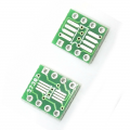
Breakout boards like the ones show in the post above are super helpful in this case. If you insist on just using wires, use a small gauge wire. Using something like 30awg wire will help avoid the solder joints from breaking so easily.
 

dl324

Joined Mar 30, 2015
16,917
I'm guessing what I need is an IC base. Solder the wires on to the base and then insert the IC.
It would be helpful if you showed us a picture or described your scenario better. When you mention "tiny pins", that would imply through hole package. But those leads aren't what most would consider tiny.

I have some surplus parts I bought that were in DIP8 and had wires soldered to the leads. I'll dig one out and post a picture. As I recall, all of the wires were running in the same direction so they could be bundled together to give some strain relief; but the wires on these weren't bundled.
 

Audioguru again

Joined Oct 21, 2019
6,691
Many beginners use a very cheap soldering iron that has no temperature control, or it has a simple "light dimmer circuit" to change the temperature but it does not control the temperature. It is WAY TOO HOT and it incinerates instead of soldering properly. My soldering iron is a Weller that has temperature control and it has been used almost every day for 52 years.
Beginners also use very cheap solder that is probably plumbers solder wrongly described as electronic solder on ebay.
 

Thread Starter

infy

Joined Jun 18, 2020
13
The IC is LME49720 Op-Amp.
specs

I'd love to have an alternative to wires. Noted on a smaller wire.

This circuit I'm building is a twin t notch filter. It will be used to take SNR/THD+N measurements of extremely low noise high performance DA converters on scopes. So I need a very clean notch circuit to keep the signal as precise as possible. I'll probably have to build a few different variants to dial in the frequency.

I'm not sure if this will work in the end with my breadboard and nest of wires. Learning as I go.
 

dl324

Joined Mar 30, 2015
16,917
The IC is LME49720 Op-Amp.
We still don't know which package you're talking about or why you think you need to use wires.

Here's a picture of the through hole part with wires attached to the leads:
1592585664964.png

Unless you think you know more than manufacturers, follow their soldering temperature and duration recommendations. They don't take the time to do that for grins. If you exceed recommendations, you may be unlucky and just make the device less reliable (vs killing it outright).
 

MrSoftware

Joined Oct 29, 2013
2,197
The IC is LME49720 Op-Amp.
specs

I'd love to have an alternative to wires. Noted on a smaller wire.

This circuit I'm building is a twin t notch filter. It will be used to take SNR/THD+N measurements of extremely low noise high performance DA converters on scopes. So I need a very clean notch circuit to keep the signal as precise as possible. I'll probably have to build a few different variants to dial in the frequency.

I'm not sure if this will work in the end with my breadboard and nest of wires. Learning as I go.
Be aware that when any noise is very significant, your power supply, power filtering parts and layout will be at least as important as the parts you choose, if not more important. Making the circuit on the breadboard can give you some idea for how it will work, but things can change, for better or worse, when you move that to a real custom PCB, and again when you integrate it with another circuit. I'm not trying to deter you, on the contrary I'm just saying if you see some unexpected behavior at some point, it could be due to things that are not obvious at first, such as layout.
 

Thread Starter

infy

Joined Jun 18, 2020
13
The power supply will be DC batteries to keep noise down.

I'm not expecting to to put this on a custom PCB. My goal is to simply assemble and take some measurements. Maybe that will change in the future though.

If I knew how to design the proper PCB I'd just spend the money and go for that :)
 

Tonyr1084

Joined Sep 24, 2015
7,899
As far as heat damage goes, I'd be more concerned with the pads the parts are being soldered to. Too much heat for too long a time can cause the pads to lift off the board. IF the board is just a bunch of annular rings on one side - heat is definitely a concern. If the pads are on both sides but no plating in the hole, heat is still a significant concern. IF the board is plated through (and I'll draw a picture in a minute or two) then the holes are more robust and less likely to lift (come off). Finally, if the pads are surface mount pads then again, heat becomes a concern.

Someone before already mentioned tacking the IC to the board. That's exactly what I do when I have wires to add to the circuit. I'll just tack one corner then the opposite corner just to hold the IC in place. Then I'll make all the wired connections I have to make, soldering each as I go. When I need to solder to the two tacked corners care becomes an issue. Take it easy and don't overheat the joints, mostly because of possible failure of the glue holding the pad in place. But even if it comes off and we're talking about a through hole part you can always wrap a small hook of wire around the lead and solder it. Remember, the other leads are soldered and should hold the IC in place.

Drawing to come shortly.
 

Tonyr1084

Joined Sep 24, 2015
7,899
Here's the drawing: The red pad indicates the copper pad or trace. The component can be an IC or a two leaded device. The gull wing SMD does not necessarily have a PTH. [edit] Oops! Should be "SMT" and not "SMTD". [end edit]

1592593664666.png
 

shortbus

Joined Sep 30, 2009
10,045
I need to solder all 8 pins to wires so I can connect the wires to the rest of the circuit.
It's been done many years ago and even today, called "dead bug" construction.
Dead bug" construction
Free-form construction can be used in cases where a PCB would be too big or too much work for a small number of components. Several methods of construction are used. At one extreme a wiring pen can be used with a perforated board, producing neat and professional results. At the other extreme is "dead bug" style, with the ICs flipped upside-down with their pins sticking up into the air like a dead insect, the leads of components are usually soldered directly to other components where possible, with many small circuits having no added wires. While it is messy-looking, free-form construction can be used to make more compact circuits than other methods. This is often used in BEAM robotics and in RF circuits where component leads must be kept short. This form of construction is used by amateurs for one-off circuits, and also professionally for circuit development, particularly at high frequencies.[4]

For high-frequency work a grounded solderable metallic base such as the copper side of an unetched printed circuit board can be used as base and ground plane. Information on high-frequency breadboarding and illustrations of dead bug with ground plane construction are in a Linear Technologies application
From - https://en.wikipedia.org/wiki/Point-to-point_construction#"Dead_bug"_construction

http://www.worldofindie.co.uk/?p=900
 

MrChips

Joined Oct 2, 2009
30,806
You don't have to make a PCB in order to get PCB performance.

Take a piece of copper clad laminate, single or double sided. With a sharp knife cut channels to create islands of copper.
Solder your components and IC legs to the islands. If you have double sided laminate, make the bottom side a ground plane.

1592617158517.png
 

Thread Starter

infy

Joined Jun 18, 2020
13
I'm actually getting very interested in the prototype PCB path. It looks pretty cheap.. At least the upfront costs I'm seeing. I can get a set of variations built and take some measurements.

I found (commercial link removed by moderator) and will give that a shot.
 
Last edited by a moderator:
Top