 Facebook
 Google
 GitHub
 Linkedin
Hello,
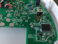
When I opened an optic smoke dedector,I saw the pcb layout of photodiode was different.
there was no pcb ink,I attached the photo.Why pcb ink has not been used?
When I opened an optic smoke dedector,I saw the pcb layout of photodiode was different.
there was no pcb ink,I attached the photo.Why pcb ink has not been used?
Attachments
-
 742.3 KB Views: 25
 )
)


