Simulating a buck-boost converter in LTspice

Thread Starter

vooper

Joined Dec 2, 2016
23
Hello again
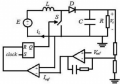
Trying not to make a new topic to ask for help, but I have revised my circuit to try and match the results that I wanted in my first post. And so I have added a current to voltage changing circuit. Added a comparator so that the switch has a peak reference value to determine when the switch opens.
I wasn't entirely sure if I was supposed to use the "srflop" function or "dflop", but I assumed that what was I needed in order to make the results I wanted.
My question this time, however, is which parameters should I be changing in order to get the results that I had been wanting in my first post?
I assumed the value for the voltage reference point would make it so that the peak current was 4A, but that didn't work.
 

Attachments

Thread Starter

vooper

Joined Dec 2, 2016
23
I wasn't entirely sure what to put for the power supplies, but after adding supplies to those components, I didn't really get results that differed from the simulation even without supplies.
One other thing I noticed was that, this simulation seems to be running in a discontinuous mode, whereas I wanted to run in a continuous current controlled mode. Are there any tips as to fix these issues?
 

Attachments

eetech00

Joined Jun 8, 2013
4,723
hi

Per Alex_T, fix the opamp/comp supply connections.

Also..
Initialize L1 to 0 current. like this:
.IC I(L1)=0

Tran statement should use "startup" option.
.tran 10m startup

Use the same power source (V1) for all power connections (including opamp/comp supply).

CM or DM will depend on how much current is being drawn by the load.
less current causes DM, more current eventually causes CM.

The topology you've used will generate a negative output voltage.

You haven't given any design requirements so how can anyone provide guidance on the design?
 

Thread Starter

vooper

Joined Dec 2, 2016
23
Reversing the polarities was just embarrassing...

I assume using the same power source would mean connecting the wires as in the circuit below?
I realize that this circuit reverses the polarity and outputs a negative voltage, and I assume that what determines the output voltage is the duty ratio of the switch. Just as a test I would like to perhaps get a voltage double of the input voltage. Though, I don't really understand how to change said duty ratio.

I'll try to be as specific as to what I was trying to recreate:
A CCM buck-boost converter using the voltage switch. Therefore I added what I assume is a current to voltage changing unit with the whole buffer, opamp bit. The comparator uses one of the voltage sources as a reference for the desired threshold current.
Have a clock frequency of 20kHz or maybe 50kHz for the switch. I assume that the R portion for the flip flop is where the clock goes and adding a source with pulse settings would recreate a clock setting.
Make the threshold current for the inductor 4A.
Make it so that when the current through the inductor reaches 4A, the current begins to fall again, until the current reaches either 0A or until the next clock pulse is input.
Not really looking to improve ripples yet, as I'm mainly just trying to focus on the current.
 

Attachments

eetech00

Joined Jun 8, 2013
4,723
HI

The digital devices default to 1v I/O, so change Vt param in SW model to this:
.model SW SW(Roff=1meg Ron=10m Vt=0.5 Vh=10m)
So that the switch turns on at V(Q)/2.
Also change Ron,Roff params so that when switch is off,
contact resistance = 1MEG, on=10milliohm (as if the switch were a power mosfet)

Also change C1 to something much larger, like 100uF, so that the output waveform has a lot less ripple. Label the junction of D1,C1,R1 as "OUT", then click this label to display the waveform.
 

Thread Starter

vooper

Joined Dec 2, 2016
23
Well I kept trying to play around with the numbers a bunch everywhere to get desired results, but unfortunately nothing even gets me close to 4A, let alone 1A across the inductor. Strangely, the simulation just stops at around 18ms and just yields 0 current after that point.
 

Attachments

crutschow

Joined Mar 14, 2008
38,668
Make it so that when the current through the inductor reaches 4A, the current begins to fall again, until the current reaches either 0A or until the next clock pulse is input.
The logic of your circuit won't do that.
Do you want the comparator to both stop the current at 4A and start the current at 0A, as well as the clock pulse starting the current?

If you want the comparator to trip at 4A you need R3 to be larger or more gain at U1.

It seems like your are somewhat randomly throwing circuits on the wall to see if they'll stick. :rolleyes:
 

Thread Starter

vooper

Joined Dec 2, 2016
23
It seems like your are somewhat randomly throwing circuits on the wall to see if they'll stick. :rolleyes:
Yeah, I'll be honest, that's basically what I'm doing.

The logic of your circuit won't do that.
Do you want the comparator to both stop the current at 4A and start the current at 0A, as well as the clock pulse starting the current?
I thought it was the flip flop's job to do that bit of storing information and determining the next clock input? Then that the comparator just sees if the current, or voltage in this case I suppose, across the inductor is greater than or less than the voltage reference, V2 in the above schematic, and outputs whatever until the voltage reaches the value of V2.
Though, yes, I suppose I do want the comparator to close the switch at 0A and open the switch upon reaching 4A, if that's its job.

I have also tried changing around the values for R3 and such, but increasing the value for R3 only seemed to decrease the maximum current flow, and changing the values for the opamp bit didn't really change anything.

I also can't seem to determine what's causing the abrupt simulation end near the 18ms mark either.
 

crutschow

Joined Mar 14, 2008
38,668
I thought it was the flip flop's job to do that bit of storing information and determining the next clock input?
The flip flop's (actually a latch in your circuit) "job" is to store whether the Set or Reset input last went high and give an output representing that, nothing more.
It has nothing to do with "determining the next clock input" whatever that means.
Though, yes, I suppose I do want the comparator to close the switch at 0A and open the switch upon reaching 4A, if that's its job.
It's up to you to decide what its "job" is, and design the circuit accordingly.
If you want the comparator to both signal 4A and 0A then you may need 1 comparator for each condition.
Note that the comparator requires a resistor pull-up to the supply voltage for proper operation (look at its data sheet).
I also can't seem to determine what's causing the abrupt simulation end near the 18ms mark either.
I wouldn't worry about that unit you get it operating as you want.

I suggest you make a timing diagram of exactly what you want to happen for all the signals and go from there.
Random design is unlikely to get you a properly working circuit.
 
Last edited:

Thread Starter

vooper

Joined Dec 2, 2016
23
If you want the comparator to both signal 4A and 0A then you may need 1 comparator for each condition.
Sorry if I'm completely misunderstanding, but doesn't having the diode prevent the current through the inductor to go below 0A anyways, and so the logic should make it so that the switch just closes when a clock pulse is input or if the current manages to hit 0?
 

Thread Starter

vooper

Joined Dec 2, 2016
23
Is it at least making the switch turn off when the current reaches the reference voltage, because that's what I had assumed it was supposed to do so?
 

crutschow

Joined Mar 14, 2008
38,668
Been looking through some papers and whatnot, and I realize this pic is of a boost converter, but is this basically not all that I need in order to reenact what I have been looking for?
If you tell us precisely and clearly what are "looking for", then we may be able to answer that question.
 

Thread Starter

vooper

Joined Dec 2, 2016
23
Sorry, English isn't my forte so I probably have not been able to convey my messages clearly.

I'll try to write down what I wanted to do in an algorithm style:
1. Create a continuous mode buck-boost converter
2. Start with the switch closed to let current flow through the inductor.
3. Take the current flowing through the inductor, and convert it into a voltage value, so that it can be used with the voltage controlled switch.
4. Compare the current through the inductor with the reference voltage, e.g. 4 (V2) from the circuit in post #28
5. If the current reaches the value of the reference voltage, turn the switch off, so that the current begins to fall again.
6. Put in a clock frequency that controls when the switch turns on. (I assumed that, Tperiod is basically the clock frequency and Ton determined how long the switch would stay on for V3 in the same circuit of post #28)
7. If the current through the inductor reaches 0, or if a clock pulse is detected, turn the switch on. (Since the clock frequency is relatively high, I don't think that the current will have time to actually reach 0, but just in case, I wanted to add it as a condition)
8. I am not looking to optimize the output voltage, but mainly focusing on the current through the inductor. I am not trying to get a uniform wave pattern. I am looking for chaos.

I hope I have been able to convey everything, but if there are still things unclear, my apologies.
 
I also had a problem with the current switch (perhaps just an error in the syntax) so I changed to the voltage controlled switch, as shown below and sensed the voltage across the 1 milliohm shunt resistor (1mV = 1A).
I also changed the output capacitor and load resistor values so it settles to a low-ripple DC output voltage.

View attachment 116262
if i want to change the input voltage to 12V, am i must change the other component's value also?
 
Top