Facebook
 Google
 GitHub
 Linkedin
Rick Martin
- Joined Jun 14, 2009
- 31
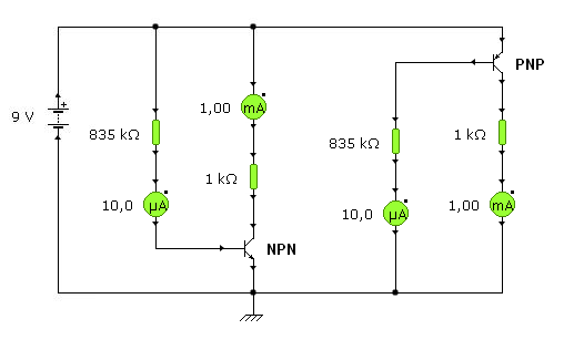
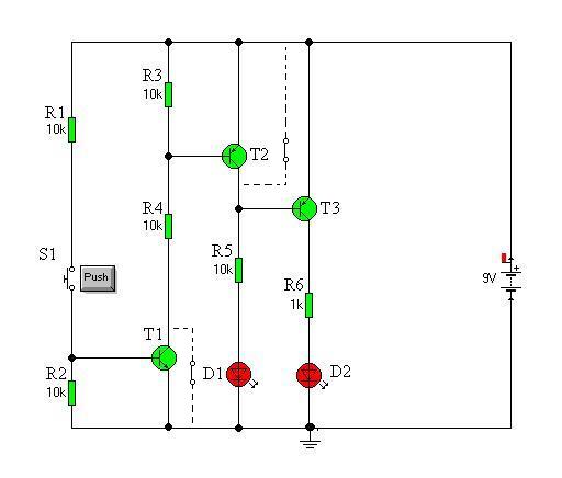
No worries mate and to your question to Jony, yes it is and it may help if you flip the diagram up side down so the emitter is on the bottom to help understand the negative relationship of the PNP (2nd pic) compared to the PNP (1st pic), but Jony will expand on that I would say.Hi Rick
Sounds good, yes I need to do some more grunt work first, almost there. Problem is I don't have a tutor, so here I am.
Jony
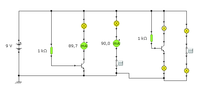
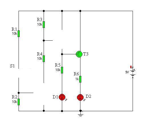
In the Q diagrams the current is coming out of the collector on the second pic. So, umm, if E is the sum of B and C how is the current being "emitted" from C
Good luck with it all mate.