 Facebook
 Google
 GitHub
 Linkedin
I am seeking some help with choosing resistor values for a high side switch circuit.
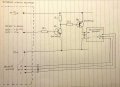
Firstly, a bit of context: I am adding a bluetooth receiver circuit to my old Sony HiFi. The bluetooth circuit (KRC-86B) comes with little information, but requires 3.3V to 5V DC supply and I have measured about 30mA maximum current draw when the device is paired. I am taking the 5V DC supply from a suitable point on the stereo main board, but have discovered that this rail is permanently at 5V, even when the stereo is in standby. I am therefore adding a simple transistor switch circuit to power up the bluetooth circuit only when the HiFi is switched on. This will be triggered by tapping off the STBY signal which enables the amplifier chips. The STBY signal goes from 0V when off to 6.9V when on.
Attached is a sketch of my proposed high side switch circuit. The transistors (2N3904 and 2N3906) are the only ones I currently have, so wish to use these unless there is a good reason not to. I'm assuming a maximum load current of say 40mA to be on the safe side and believe that the transistors have a modest saturated gain of about 10. I can estimate R3 at about 1k to give a Q2 base current of about 4mA (40mA/10) but am struggling to know how best to calculate the other two and not sure if R2 is even required??
Any advice would be gratefully received, specifically on whether I'm on the right track, how to calculate the resistor values and the necessity of R2.
Attachments
-
 114 KB Views: 24


