Facebook
 Google
 GitHub
 Linkedin
Hi,
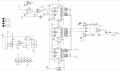
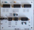
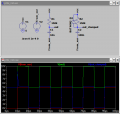
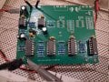
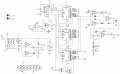
In this article near the bottom there's FIR filter. I'd like to understand how the resistor values are calculated.
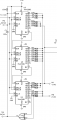
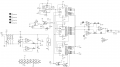
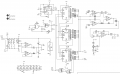
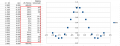
Schematic
When I naively do 26.75k/sinc I get roughly the right values but not quite good enough. Any ideas on how this is done?
In this article near the bottom there's FIR filter. I'd like to understand how the resistor values are calculated.
Schematic
When I naively do 26.75k/sinc I get roughly the right values but not quite good enough. Any ideas on how this is done?
Attachments
-
 52.8 KB Views: 36