 Facebook
 Google
 GitHub
 Linkedin
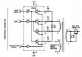
Hello - New to this website and forum and hoping that I have posted in the correct location. I have a question on the attached diagram from a datasheet for an IBM protocol converter chipset (DP8340 Transmitter and DP8341 Receiver). These two chips work in conjunction with a DS3487 Quad Tri-State Line driver to connect to coax line to transmit and receive data. The receiver simply connects to the coax via the 1:1:1 transformer. However, the transmitter as shown in the sample application uses several resistors (R1 thru R5) before going to the transformer. The Data Delay and Data lines are inverse of each other and driven by the output of the transmitter. I understand pin 4 controlling the Hi-Z state but do not understand the function and values of the resistors. I have a very rudimentary understanding of electronics and I am trying to understand the purpose of the resistors. From the chipset datasheets, the Data Delay and Data (inverted) appear to be identical but inverted. So I am confused on the not only the purpose of the resistors, but also why the difference in chosen values of 150 for Data and 33 for the Data Delay logic. My guess on the receiver is that the resistance values may be built into the chip and that is why there is a direct connection to that chip from the coax. I would like to understand the concept prior to building, instead of simply assembling components. Thank you for your time in reviewing this post and I very much appreciate any helpful information.
Attachments
-
 259.2 KB Views: 21


