Request for Explanation of Clicker Circuit Functionality

Thread Starter

joerock

Joined Jun 16, 2024
6
Hi,

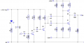
I have a clicker circuit for interacting with a smartphone, as shown in the attached picture. Electrodes A and B are used to affect the capacitance on the phone's screen. Could you please explain how this works?

Thank you very much.
 

Attachments

MisterBill2

Joined Jan 23, 2018
27,193
It appears that the circuit uses what looks like half of an "H bridge" to reverse the polarity of the voltages at points "A" and "B".
But how that actually interacts with a touch screen is not clear to me, either.
 

Thread Starter

joerock

Joined Jun 16, 2024
6
It appears that the circuit uses what looks like half of an "H bridge" to reverse the polarity of the voltages at points "A" and "B".
But how that actually interacts with a touch screen is not clear to me, either.
Dear MisterBill2, Thank you for your reply. This circuit is a clicker unit that works with a smartphone screen. Electrodes A and B are used to affect the capacitance on the phone's screen, simulating a human finger. Here is the original youtube video for reference:
 
The A input senses a signal from screen (very low level) and triggers a Q4&Q3 amplifier.
So at Q3 collector appears a pulse.
This pulse generate a high voltage bipolar pulse (-20V/+20V) on B.
The pulses A and B are inverted each other.
 
Last edited:

Thread Starter

joerock

Joined Jun 16, 2024
6
The A input senses a signal from screen (very low level) and triggers a Q4&Q3 amplifier.
So at Q3 collector appears a pulse.
This pulse generate a high voltage bipolar pulse (-20V/+20V) on B.
The pulses A and B are inverted each other.
Dear Michal Podmanický,

Thank you very much for the information. However, I am a bit confused about how Q1 and Q2 work, and also about the use of ±20V. From the circuit, when electrode touches the smartphone display at point A, the resistance of the display changes. This resistance change affects the current flow through R13, and the current is amplified by transistors Q3 and Q4. This results in Q1 turning on. From this point onward, I am not sure how the next functions proceed.

Could you please explain how Q1 and Q2 operate in this circuit, and the role of the ±20V supply?

Additionally, it would be helpful to know what the signal looks like at each stage:

Q4 base and collector
Q3 base and collector
Q1 base and collector
Q2 base and collector
Thank you!
 
Q1 is npn and Q2 pnp connected in common emitter configuration. The marking on schematic is wrong.

Q3 & Q4 are sets to have a very high gain, so even small signal on A is able to generate a square wave at Q3 collector.

Once a positive pulse is applied to A a Q4 collector goes down and Q3 collector goes up, so Q1 fully open (conduct) and Q2 fully closes (not conduct). This causes a -20V appears on B. The C5 just removes a DC component of +-20V signal.

When input signal on A disappeare (or even goes negative), the Q4 collector goes up, the Q3 collector to gnd, what causes Q1 fully closes and Q2 fully opens. A +20V appears on B.

This is a correct output connection:
IMG_0858.jpeg
 
Last edited:

Thread Starter

joerock

Joined Jun 16, 2024
6
Q1 is npn and Q2 pnp connected in common emitter configuration. The marking on schematic is wrong.

Q3 & Q4 are sets to have a very high gain, so even small signal on A is able to generate a square wave at Q3 collector.

Once a positive pulse is applied to A a Q4 collector goes down and Q3 collector goes up, so Q1 fully open (conduct) and Q2 fully closes (not conduct). This causes a -20V appears on B. The C5 just removes a DC component of +-20V signal.

When input signal on A disappeare (or even goes negative), the Q4 collector goes up, the Q3 collector to gnd, what causes Q1 fully closes and Q2 fully opens. A +20V appears on B.

This is a correct output connection:
View attachment 324930
I am truly grateful for your kindness and effort. May you always be blessed with happiness and good health.
 

MisterBill2

Joined Jan 23, 2018
27,193
After all of the schematics are corrected, I would be very interested in knowing if the circuit is actually able to produce the desired results of simulating finger touches on the touch keypad.
 

Thread Starter

joerock

Joined Jun 16, 2024
6
After all of the schematics are corrected, I would be very interested in knowing if the circuit is actually able to produce the desired results of simulating finger touches on the touch keypad.
Yes, it worked. I extracted the circuit from the clicker and found four wires: green, red, white, and black. The green wire is the trigger, the red wire is +20V, the white wire is -20V, and the black wire is ground. To operate it, you need to supply ±20V and pass the signal from the Arduino to the trigger wire for at least 50ms (calculated from RC=470kΩ×100nF=47ms). The reason for supplying ±20V and rapidly reversing it is to create an EMS change that will be detected by the phone's controller.

This is principle
principle.png

The results are shown in my video.
 

MisterBill2

Joined Jan 23, 2018
27,193
I SEE! From the explanation we learn that a trigger pulse magically causes a filed reversal that somehow simulates a finger touch alteration of the electrical field produced by the sensing circuit. Not quite the level of detail I was hoping for.
 
Top