Reduce current through FETs for Push Pull Converter

Thread Starter

artmaster547

Joined Jan 6, 2016
409
Hi
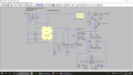
All with the assistance of a few people I have designned a push pull converter that takes in 12V and outputs +175V and -175V, however one of the main issues I am having is with the current of the FETs they are really large in the magnitudes of 500A for some FETs I have tried changing to different FETs but the current still seems incredible large, I will be delivery 375W to the load I think at the moment It's designned for 300W. Any pointers or help would be greatly appreciated, I have used LTSpice libraries found at:

https://forum.allaboutcircuits.com/...nents-models-of-ltspice-free-download.133690/

For a lot of the parts, I have also attached a screenshot.

Any help/pointers to improve this would be greatly appreciated.

Kind Regards

Art
 

Attachments

Dodgydave

Joined Jun 22, 2012
11,303
Your transformer doesn't have it's CT connected to the positive rail, R5 isn't connected to the output rail for the Tl431.
 

Bordodynov

Joined May 20, 2015
3,180
To reduce the maximum current, it is advisable to use a dedicated two-stroke microcircuit (for example ucc38084), which has a current limiting circuit (which removes the signal from the current sensor). And applying inductance in the transformer circuit. However, the requirements to the breakdown voltage of transistors are rising. This requires the use of damper chains and voltage limiters. Then the maximum current will not exceed the rated current more than three times.
2018-03-21_13-52-27.png
 

Thread Starter

artmaster547

Joined Jan 6, 2016
409
To reduce the maximum current, it is advisable to use a dedicated two-stroke microcircuit (for example ucc38084), which has a current limiting circuit (which removes the signal from the current sensor). And applying inductance in the transformer circuit. However, the requirements to the breakdown voltage of transistors are rising. This requires the use of damper chains and voltage limiters. Then the maximum current will not exceed the rated current more than three times.
View attachment 148770
Apologies this has to be run in alternate solver mode didn't notice this before, I have a question though about the transformer why is the input voltage placed at the centre and both sides of the transformer on the primary end?
 
Last edited:

Bordodynov

Joined May 20, 2015
3,180
Apologies this has to be run in alternate solver mode didn't notice this before, I have a question though about the transformer why is the input voltage placed at the centre and both sides of the transformer on the primary end?
Difficulties of translation. Formulate your question differently. I did not understand what you are asking.
 

Thread Starter

artmaster547

Joined Jan 6, 2016
409
Difficulties of translation. Formulate your question differently. I did not understand what you are asking.
Sorry please ignore the previous comment what I wanted to ask is how I can adapt this schematic so that the output voltage is constant regardless of the load i.e. if there is no load there is still an output voltage of +175V and -175V, if only half the load is present then there is an output of +175V and -175V or at full load (375W) the output is also still +175V and -175V.
 

Thread Starter

artmaster547

Joined Jan 6, 2016
409
Difficulties of translation. Formulate your question differently. I did not understand what you are asking.
Also when measuring the input voltage it doesn't read 12V its much higher does this mean that nothing else that is rated for 12V can't be used with this voltage? I want to connect other components separately to this same 12V input?
 

Bordodynov

Joined May 20, 2015
3,180
Sorry please ignore the previous comment what I wanted to ask is how I can adapt this schematic so that the output voltage is constant regardless of the load i.e. if there is no load there is still an output voltage of +175V and -175V, if only half the load is present then there is an output of +175V and -175V or at full load (375W) the output is also still +175V and -175V.
Try changing the load resistance and see what voltage is produced. Also change the input voltage and see what voltage is produced. Note that changing the output voltage by 1.7 volts (when changing the input voltage and load) is about 1%, which is very good (in my opinion).
Also note that the peak sound factor can be considered about three. Unless, of course, you make a siren. And there is no need to require a source of 375 watts of continuous power.
 

Thread Starter

artmaster547

Joined Jan 6, 2016
409
Try changing the load resistance and see what voltage is produced. Also change the input voltage and see what voltage is produced. Note that changing the output voltage by 1.7 volts (when changing the input voltage and load) is about 1%, which is very good (in my opinion).
Also note that the peak sound factor can be considered about three. Unless, of course, you make a siren. And there is no need to require a source of 375 watts of continuous power.
Sorry I don't follow so the output voltage should be fixed with this design I will check again to make sure that is the case. By sound factor do you mean that this topology will create a high pitch loud noise? From the brief I have been given for this project I was told to design it to deliver 375W (it was previously 300W) can you please confirm these for me? I would really appreciate help with this, can you source the FETs for me please for this topology I am a little unsure on what should choose to be able to deliver 375W, package wise anything can be used doesn't need to be surface mount and doesn't have a height constraint. Please Art
 

Thread Starter

artmaster547

Joined Jan 6, 2016
409
Try changing the load resistance and see what voltage is produced. Also change the input voltage and see what voltage is produced. Note that changing the output voltage by 1.7 volts (when changing the input voltage and load) is about 1%, which is very good (in my opinion).
Also note that the peak sound factor can be considered about three. Unless, of course, you make a siren. And there is no need to require a source of 375 watts of continuous power.
I am just stepping through different loads now the output voltage doesn't seem to be the same across all loads
 

Attachments

ebp

Joined Feb 8, 2018
2,332
130 A peak primary current is an appalling level for an average of about 60 A.

Is there some compelling reason for not using inductors in the secondary circuit? This appears to be an attempt at a current-fed primary, but the series inductance is far too small.
 

Thread Starter

artmaster547

Joined Jan 6, 2016
409
130 A peak primary current is an appalling level for an average of about 60 A.

Is there some compelling reason for not using inductors in the secondary circuit? This appears to be an attempt at a current-fed primary, but the series inductance is far too small.
Could you show an adapted Ltspice file of this simulation with a better current? How could it be improved to reduce the current?
 

ebp

Joined Feb 8, 2018
2,332
The basic push pull converter is simply a transformer-isolated buck converter that requires two energy storage devices - an inductor and a capacitor. The transformer gives the opportunity to change the voltage, and there is a frequency doubling if a bridge rectifier is used, but it is still basically a buck converter.

Inductors are required in the output between the rectifier(s) and the capacitor(s). Without them the current will be "unlimited." Consult any standard example of a push pull converter. This one differs only due to having dual outputs, but that simply means two inductors are used. The secondary circuit is identical to that used for any ordinary full wave bridge rectifier except that inductors are placed between the [+] and [-] outputs and their respective capacitors.

As will all switchers, the equation that rules everything is δi/δt = V/L - again exactly as it is for a buck converter except that a transformer intervenes. Typically the inductance would be chosen for peak to peak ripple current of something around 30% of the average current. For 350 volts into 200 ohms, the average output power would be 613 W. At 12 volts that is 51 A. Allowing for 85% efficiency (perhaps too high), 85% max normal duty cycle (perhaps too high) and 115% peak, it comes to about 82 amperes, peak. Each FET in a push-pull will see that current but at half the maximum duty cycle, for around 46 A RMS for each FET.

A current-fed push-pull, which places the inductance in the primary circuit as in the simulation, has its pros and cons. It is not a particularly popular topology.

Be warned. There is a huge difference between a simple simulation and a real switcher. One of the things I note in the simulation is evidence of a very severe dynamic problem. Achieving good DC regulation is pretty trivial. Getting good dynamic performance is something else altogether.
 

Thread Starter

artmaster547

Joined Jan 6, 2016
409
Is there also a way to add an external shutdown feature i.e. some kind of FET that turns of the higher voltage output via a signal from an isolated Microcontroller. If also wanted to check is the 12V used for this circuit suitable to power other smaller voltage circuits i.e. microcontroller using other smaller power regulators/non isolated DCDC converters?
 

Thread Starter

artmaster547

Joined Jan 6, 2016
409
The basic push pull converter is simply a transformer-isolated buck converter that requires two energy storage devices - an inductor and a capacitor. The transformer gives the opportunity to change the voltage, and there is a frequency doubling if a bridge rectifier is used, but it is still basically a buck converter.

Inductors are required in the output between the rectifier(s) and the capacitor(s). Without them the current will be "unlimited." Consult any standard example of a push pull converter. This one differs only due to having dual outputs, but that simply means two inductors are used. The secondary circuit is identical to that used for any ordinary full wave bridge rectifier except that inductors are placed between the [+] and [-] outputs and their respective capacitors.

As will all switchers, the equation that rules everything is δi/δt = V/L - again exactly as it is for a buck converter except that a transformer intervenes. Typically the inductance would be chosen for peak to peak ripple current of something around 30% of the average current. For 350 volts into 200 ohms, the average output power would be 613 W. At 12 volts that is 51 A. Allowing for 85% efficiency (perhaps too high), 85% max normal duty cycle (perhaps too high) and 115% peak, it comes to about 82 amperes, peak. Each FET in a push-pull will see that current but at half the maximum duty cycle, for around 46 A RMS for each FET.

A current-fed push-pull, which places the inductance in the primary circuit as in the simulation, has its pros and cons. It is not a particularly popular topology.

Be warned. There is a huge difference between a simple simulation and a real switcher. One of the things I note in the simulation is evidence of a very severe dynamic problem. Achieving good DC regulation is pretty trivial. Getting good dynamic performance is something else altogether.
Wow thanks for that explanation would you by any chance be able to add this to the simulation file so I know what value inductors to us, you mentioned about dynamic performance what can I add for this to ensure that when I design a PCB based on this it will work with little intervention.
 

ebp

Joined Feb 8, 2018
2,332
I don't have LTSpice and have no interest in installing it. I don't do electronics anymore.

Designing frequency compensation for good dynamic response is not trivial and depends heavily on the characteristics of the filter capacitor. If you use peak current mode control, the output filter has only one pole rather than two as in voltage mode control. This makes the objective of passing through unity loop gain with a slope of -1 and a decent amount of phase margin somewhat easier.

I would not regulate to an auxiliary winding if good DC regulation is required. It is reasonably workable with a current fed topology but performs poorly with inductors in the secondary. In any case, it is just another winding to design, though at 175 volts output the extra winding as just a low-voltage supply could reduce power waste in the drive circuit for an optocoupler.

Outside of textbooks on the topic, Texas Instruments, primarily because of their acquisition of Unitrode, is a good source for information on switcher design. Linear Tech is also worth checking.

If the first cut of a circuit board works, you'll be exceptionally lucky. Just as an example, I once did a design where I had copper ground plane for the control circuit. Because I was using heavy copper ("4 ounce" = approx 0.0056" = 0.14 mm) I didn't allow copper between the pins on a DIP IC - the narrow necks are a bit of a problem. I fought with the thing for many, many hours with what looked like loop stability issues. The problem went away with ground copper between the IC pins. At the currents you contemplate you will need very heavy copper and/or a multilayer board with layers "sewn" together for current handling. Multilayer can be very helpful with the critical need to minimize loop areas in the power paths.

I don't know what you contemplate for the transformer. I had a certain fondness for PQ cores which are well designed in terms of making useful compromises of the many conflicting requirements. I would consider foil for the primary, though if the total number of turns is low enough there may be merit in litz wire. Any way you look at it you'll need a lot of copper.
 

Thread Starter

artmaster547

Joined Jan 6, 2016
409
I don't have LTSpice and have no interest in installing it. I don't do electronics anymore.

Designing frequency compensation for good dynamic response is not trivial and depends heavily on the characteristics of the filter capacitor. If you use peak current mode control, the output filter has only one pole rather than two as in voltage mode control. This makes the objective of passing through unity loop gain with a slope of -1 and a decent amount of phase margin somewhat easier.

I would not regulate to an auxiliary winding if good DC regulation is required. It is reasonably workable with a current fed topology but performs poorly with inductors in the secondary. In any case, it is just another winding to design, though at 175 volts output the extra winding as just a low-voltage supply could reduce power waste in the drive circuit for an optocoupler.

Outside of textbooks on the topic, Texas Instruments, primarily because of their acquisition of Unitrode, is a good source for information on switcher design. Linear Tech is also worth checking.

If the first cut of a circuit board works, you'll be exceptionally lucky. Just as an example, I once did a design where I had copper ground plane for the control circuit. Because I was using heavy copper ("4 ounce" = approx 0.0056" = 0.14 mm) I didn't allow copper between the pins on a DIP IC - the narrow necks are a bit of a problem. I fought with the thing for many, many hours with what looked like loop stability issues. The problem went away with ground copper between the IC pins. At the currents you contemplate you will need very heavy copper and/or a multilayer board with layers "sewn" together for current handling. Multilayer can be very helpful with the critical need to minimize loop areas in the power paths.

I don't know what you contemplate for the transformer. I had a certain fondness for PQ cores which are well designed in terms of making useful compromises of the many conflicting requirements. I would consider foil for the primary, though if the total number of turns is low enough there may be merit in litz wire. Any way you look at it you'll need a lot of copper.
To reduce the maximum current, it is advisable to use a dedicated two-stroke microcircuit (for example ucc38084), which has a current limiting circuit (which removes the signal from the current sensor). And applying inductance in the transformer circuit. However, the requirements to the breakdown voltage of transistors are rising. This requires the use of damper chains and voltage limiters. Then the maximum current will not exceed the rated current more than three times.
View attachment 148770

Is this what you mean by putting inductor between the recitifer diodes and output capacitors? With regards to the transformer this is going to be made by a company that specialises in this all I have to give them is the turns ratio, power and switching frequency. I changed to a simple transformer model in LTSpice I had to change the sense resistor to 0.5m.

Kind Regards

Art
 

Attachments

Last edited:

ebp

Joined Feb 8, 2018
2,332
No. The filters immediately after the rectifiers must be LC.
Disconnect the right side of C9 from the net +175V and insert an inductor.
Disconnect the left side of C10 from -175V and insert an inductor.

I don't know what your switching frequency is supposed to be, but 2.2 µF for filtering is minuscule unless it is very high or the inductances are very high (which makes peak current mode control nearly impossible). If you want to "polish" the output, put the high value capacitors right after the rectifiers and the low value after the added inductors. Note that using significant inductance, as opposed to just lossy ferrite beads, will add two more poles to the power path transfer function, which makes achieving adequate phase margin extremely difficult unless the poles are well above the unity gain crossover frequency. There is definite merit to good quality film capacitors for the main filter, but you must consider the ripple due to charge and discharge current. Good film caps will have low ESR so that concern may be greatly reduced.
 

Thread Starter

artmaster547

Joined Jan 6, 2016
409
To reduce the maximum current, it is advisable to use a dedicated two-stroke microcircuit (for example ucc38084), which has a current limiting circuit (which removes the signal from the current sensor). And applying inductance in the transformer circuit. However, the requirements to the breakdown voltage of transistors are rising. This requires the use of damper chains and voltage limiters. Then the maximum current will not exceed the rated current more than three times.
View attachment 148770
I
No. The filters immediately after the rectifiers must be LC.
Disconnect the right side of C9 from the net +175V and insert an inductor.
Disconnect the left side of C10 from -175V and insert an inductor.

I don't know what your switching frequency is supposed to be, but 2.2 µF for filtering is minuscule unless it is very high or the inductances are very high (which makes peak current mode control nearly impossible). If you want to "polish" the output, put the high value capacitors right after the rectifiers and the low value after the added inductors. Note that using significant inductance, as opposed to just lossy ferrite beads, will add two more poles to the power path transfer function, which makes achieving adequate phase margin extremely difficult unless the poles are well above the unity gain crossover frequency. There is definite merit to good quality film capacitors for the main filter, but you must consider the ripple due to charge and discharge current. Good film caps will have low ESR so that concern may be greatly reduced.
Is this correct now:
 

Attachments

Top