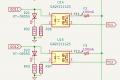
R800C and Blue pill schematic

panic mode

Joined Oct 10, 2011
5,172
no headers? how is this supposed to interface to outside world?
no buttons or jumpers or dipswitches? how do you plan to controlling startup mode?
LEDs with 47 Ohm series resistors? that is asking for massive current from GPIO (25mA-ish).
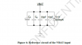
several hundred of uF across battery?
5V zener across battery? how are you planning on charging the battery?
 

Thread Starter

tomyF

Joined Jan 28, 2026
5
> no headers? how is this supposed to interface to outside world?
Connectors have headers to connect to

> no buttons or jumpers or dipswitches? how do you plan to controlling startup mode?
The device/board is not to be programmed often; mostly it's merely once
I changed my mind a little and connected both NRST and BOOT0 via a cap and resistor (respectively) to GND.

> LEDs with 47 Ohm series resistors? that is asking for massive current from GPIO (25mA-ish).
I'm going to use a LED Red 620-630nm 0805 25mA 60mW (XL-2012SURC) with a 68 Ω resistor for both LEDs in my design.

> 5V zener across battery?
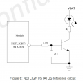
yes, below is from the SIM's hardware design
Capture.PNG

> how are you planning on charging the battery?
The battery will be charged using a li-ion 18650 (with protection) module connected to it
 
J3 already gives you 3.3V, SWDIO and SWCLK, so you do have an SWD programming connection.

It looks like pin 4 of J3 is currently unused. I would connect that pin to GND, because the ST-Link and the target board need a common ground reference. I would also consider adding NRST as a separate test pad. It is not always required, but it can be useful if the firmware makes a normal debug connection difficult.

Since NRST is already routed to the reset button, adding a test pad should be easy. With those connections, I don't think a USB connector is necessary just for programming the STM32.
 

Thread Starter

tomyF

Joined Jan 28, 2026
5
J3 already gives you 3.3V, SWDIO and SWCLK, so you do have an SWD programming connection.

It looks like pin 4 of J3 is currently unused. I would connect that pin to GND, because the ST-Link and the target board need a common ground reference. I would also consider adding NRST as a separate test pad. It is not always required, but it can be useful if the firmware makes a normal debug connection difficult.

Since NRST is already routed to the reset button, adding a test pad should be easy. With those connections, I don't think a USB connector is necessary just for programming the STM32.
Thanks for your points.

Below is my new design. Pin4 of J3 is (already) connected to GND and I connected both NRST and BOOT0 to GNd since the device is (mostly) programmed only once.
 

Attachments

panic mode

Joined Oct 10, 2011
5,172
Connectors have headers to connect to
so where are they on schematics? how are you exposing IO pins? i am expecting to see some 2x 20pin

I'm going to use a LED Red 620-630nm 0805 25mA 60mW (XL-2012SURC) with a 68 Ω resistor for both LEDs in my design.
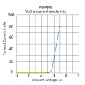
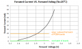
did you read the datasheet for STM32F1? are you sure PC13 can source 25mA? even if it can it is a bad idea. you do not want to stress or load the most complex part on your board, that is job for transistors. same with LED datasheet. what made you pick 25mA? this is just an indicator, not a flashlight. besides,, datasheet clearly says that breaking point (absolute maximum) for this LED is 20mA, so how in the world did you decide to choose 25mA?

and red LED will have Vf about 1.6-1.7V so

(Vgpio-Vf)/If = (3.3V-1.7V)/5mA= 320 Ohm. the nearest common value is 330 Ohm.

below is from the SIM's hardware design
View attachment 370536
ok, zener stays, what about those caps? bypass caps are parallelled to reduce impedance over wide frequency spectrum. so those capacitors need to be different (small, medium, large,...).
the datasheet shows that small value caps are in pF range.the smallest cap you use us 0.1uF.

The battery will be charged using a li-ion 18650 (with protection) module connected to it
that is also not shown in schematics. if this is a BluePillas you call it, i expect to see 2x 20pin. but your schematics shows only couple of pins on J1, J2 and J8.
 

panic mode

Joined Oct 10, 2011
5,172
you should have started by posting your own links to datasheets so people willing to help do not have to navigate minefields of clickbait and malicious downloads.
for example R800c datasheet:
https://www.eevblog.com/forum/begin...ue-pill-board/?action=dlattach;attach=2713183

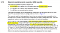
but this is incomplete. for detailed electrical specs you need to keep searching. then you will find that absolute max Sink/Source current is only 2mA per pin. so you should never drive LED directly by some IO pin. that LED on pin 41 is a short circuit as far as R800C is concerned.
 
Top