 Facebook
 Google
 GitHub
 Linkedin
Hi,
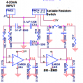
I am programming a c8051F850 to take in both a potentiometer and a 4-20mA current loop input through a ADC (0-3.3v mapped to 0-1023 10-bit range). However not being a electronics/board design engineer i would appreciate some help on the following circuit (see attached schematic). I read P1.3 with potentiometer input (from J12 with pin 2 not being used) and everything works ok. However i am not quite clear on how the current loop input (from J11) gets mapped to my expected 0-1023 range within the program. As i understand from the schematic, the 4-20mA input is sent over a 10ohm resistor thus converting it to a 40-200mV range (subset of the 0-3300mV range the ADC is configured for) and thence to a subset of the 0-1023 range to pin P1.0. Is my understanding correct? What then is the circuit on P1.1? How is it related to the circuit on P1.0?
--Ram
Attachments
-
 79.2 KB Views: 48
")


