 Facebook
 Google
 GitHub
 Linkedin
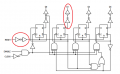
Attached is a digital circuit of the MC14518B.
What's the real meaning of that combination in the red circle? Would it be like a buffer? I mean, the input is being inverted, then goes to another not gate with the bubble at the input. Would it be the same if I just put the normal gate symbol instead?
What's the real meaning of that combination in the red circle? Would it be like a buffer? I mean, the input is being inverted, then goes to another not gate with the bubble at the input. Would it be the same if I just put the normal gate symbol instead?
Attachments
-
 34.1 KB Views: 32


