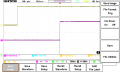
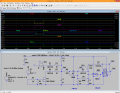
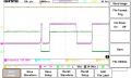
Q2/ is pin12 of U2 ,Q1 is pin1 of U2
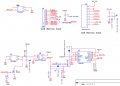
Please see the attached circuit in the above post.
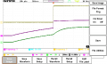
Channel 1 yellow is PWR_BTN
Channel 3 Red is Q1
Channel 4 Green is Q2/ STB_CTRL
...............
Sometimes Q2/ can not change status.
If I zoom in the waveform.
I found some glitch on Q1, so STB_CTRL change unnormally.
I do not know why there is glitch on Q1?
Could you help to solve this problem?
Thanks
Best regards
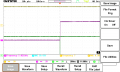
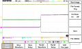
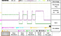
The upload file is some waveform.
Channel 1 yellow is PWR_BTN
Channel 3 Red is Q1
Channel 4 Green is Q2/ STB_CTRL
Sometimes Q2/ can not change status.
If I zoom in the waveform.
I found some glitch on Q1, so STB_CTRL change unnormally.
I do not know why there is glitch on Q1?
? Clock 2 is tied to PWR Button
? Q1 is forced to reset from +5V (Reset1 generates an unpredictable disruption to outp Q1 = Low )
? ↑ is this the circuit you measure ↑ (chk your circuit wiring + logic + relative controls timing)
? What kind of supply (+filter caps near CD4013) and what is the probe
there is no functionality you describe
= provide a correct circuit you measure with scope !!!
Crutschow ? your schematic is somewhat suspicous
this is how i got it to do something (but this is not a good way of doing this)
? what's your simulator
___________
quick mod
Suspicious how?
The CD4013 data sheet shows that with both the PRE and CLR inputs high, Q-out is high, so I don't see that your change for the CLR input makes a difference.
Also your change to the CLR input for A2 means the it will power up with the output transistor on.
Why did you change that?
you might be right
______________
however the OP has a slightly different circuit
the cause of output instability is likely the missing 100nF
but it might also be a non std. use of S R by Crutchow . . . (or a speciffic scope & probe used . . .)
? Clock 2 is tied to PWR Button
? Q1 is forced to reset from +5V (Reset1 generates an unpredictable disruption to outp Q1 = Low )
? ↑ is this the circuit you measure ↑ (chk your circuit wiring + logic + relative controls timing)
? What kind of supply (+filter caps near CD4013) and what is the probe
there is no functionality you describe
= provide a correct circuit you measure with scope !!!
i managed to simulate the case . . . but hadn't time yet to track it down (so hold your horses a bit)
. . . what we can tell at this point is that the bug is not present at non-inverting outp
so you may Reset your Latch-2 instead of Set and use the non-inverting Q2 outp for control/strobe
____________
it's occuring at rising Clock slope (the trace Vp3 = Clk , Vp4 = ¯Q2 , Vp6 = Q2)
the bug is likely inside the logic of the chip ?? (K -- non-inverting OUTP , M -- inverting)
_________
? a fix
Q2/ is pin12 of U2 ,Q1 is pin1 of U2
Please see the attached circuit in the above post.
Channel 1 yellow is PWR_BTN
Channel 3 Red is Q1
Channel 4 Green is Q2/ STB_CTRL
...............
Sometimes Q2/ can not change status.
If I zoom in the waveform.
I found some glitch on Q1, so STB_CTRL change unnormally.
I do not know why there is glitch on Q1?
Could you help to solve this problem?
Thanks
Best regards
I used 1/2 of the CD4013 FF as a buffer circuit (in a somewhat unconventional configuration) to give a fast rise-time clock pulse to the second toggle FF, without having to add another IC.
But if that circuit is glitching, then two CD40106 Schmitt trigger inverters can be used in series as a substitute, eliminating the chance of generating a glitch (circuit below).
Here's an alternate circuit. It uses two chips but is flexible. See below.
This uses a Schmitt trigger inverter to clock the CD4013B, so shouldn't be affected by slow RC rise times.
It also use a mosfet at the output to reduce the output current requirement of the CD4013B.
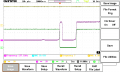
I just go to office now.
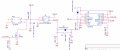
My circuit is as attached file.
C7 is capacitor near CD4013B.
I add another capacitor on VDD of CD4013B.
The result is the same.
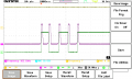
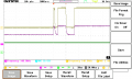
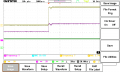
The channel 1 Yellow is PWRBTN.
The channel3 Red is Q1 of U2.
The channel4 Green is Q2/ of U2.
I have cutoff the Q2/ to other circuits.
So Q2/ can not be affected by other circuits.
The first 2 picture is normal waveform.
When I push the button, Q1 change to high, and Q2/ toggle.
The last 7 pictures is unnormal waveform.
The Q1 toggle unnormally many times.
So Q2/ toggle because of Q1 toggle.
I do not know why Q1 toggle often?????
I just go to office now.
My circuit is as attached file.
C7 is capacitor near CD4013B.
I add another capacitor on VDD of CD4013B.
The result is the same.
The channel 1 Yellow is PWRBTN.
The channel3 Red is Q1 of U2.
The channel4 Green is Q2/ of U2.
I have cutoff the Q2/ to other circuits.
So Q2/ can not be affected by other circuits.
The first 2 picture is normal waveform.
When I push the button, Q1 change to high, and Q2/ toggle.
The last 7 pictures is unnormal waveform.
The Q1 toggle unnormally many times.
So Q2/ toggle because of Q1 toggle.
I do not know why Q1 toggle often?????
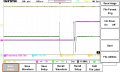
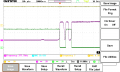
I cutoff the second circuit D flip flop of CB4013B.
Only measure the first D flip flop.
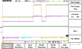
Channel 1 Yellow is Q1.
Channel 3 Red is Negative side of D1
Channel4 Green is SET of U2.
The first waveform looks normally.
If I zoom in the waveform.
The last other waveform sometimes looks unnormal.
The Q1 will fall down to 0V ??????
I do not know why Q1 down to 0V.
I do not use the second D flip flop.
Q1 will not be affected by second D flip flop.
Why ?
Gave an upvote for #36 -- not because it's essentially correct -- but because you took a stand to more freely came up with your own solution
/// the problem with our help is that we do and find the first thing that may more or less meet your design requirements -- but without knowing the exact details of it -- only you can verify what it is actually to be
_____________________
 Facebook
 Google
 GitHub
 Linkedin