I'm making a large circuit involving multiple IC's both digital and analog. Some components will be running at 20Mhz (processor), some at around 500Mhz maximum (radio), and others at substantially lower frequencies.
I learned that to minimize chances of EMI, I need to decouple the power supply, so noise from one circuit doesn't run to the next.
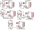
What I have attached is a small fragment of my design in different versions. The power supply is shared amongst all IC's. The inputs (1st, 2nd 3rd) are address lines connected to the microprocessor. These lines get updated roughly 100 times a second. The data line (D) is updated at least 100,000 times a second.
I'm trying to figure out which version is best to use.
the first one at top-left is coupling I think most people use (+ve runs through resistor and gets shunted by capacitor). If I use this method, the circuit board will not be routable. I'm limited to single-sided PCBs.
The second method (top right) is bad as noise can freely enter the circuit, so I see no advantage to it.
The next one (middle-left) is the same as first except I'm applying the filter to a chip input. (I'm not sure if failing to do this causes the chip to emit noise via inputs?)
The second last one (middle-right) is the same as middle-left but I did the coupling on the negative side as well.
The last one is similar except I connected -ve to the G2 inputs on the chip directly.
If I use the last or 2nd last circuit, routing will be substantially easier on a single sided board without requiring jumpers.
Assume for all circuits that each resistor is 10 ohms 1/4 watt, and each capacitor is an electrolytic 100uF rated for 16 volts, and each battery provides 5VDC of unregulated power (for sake of argument, lets say its 4 1.2V cells in series.)
Apart from what I mentioned, are there any benefits or drawbacks to using any of the five methods I have shown?
I learned that to minimize chances of EMI, I need to decouple the power supply, so noise from one circuit doesn't run to the next.
What I have attached is a small fragment of my design in different versions. The power supply is shared amongst all IC's. The inputs (1st, 2nd 3rd) are address lines connected to the microprocessor. These lines get updated roughly 100 times a second. The data line (D) is updated at least 100,000 times a second.
I'm trying to figure out which version is best to use.
the first one at top-left is coupling I think most people use (+ve runs through resistor and gets shunted by capacitor). If I use this method, the circuit board will not be routable. I'm limited to single-sided PCBs.
The second method (top right) is bad as noise can freely enter the circuit, so I see no advantage to it.
The next one (middle-left) is the same as first except I'm applying the filter to a chip input. (I'm not sure if failing to do this causes the chip to emit noise via inputs?)
The second last one (middle-right) is the same as middle-left but I did the coupling on the negative side as well.
The last one is similar except I connected -ve to the G2 inputs on the chip directly.
If I use the last or 2nd last circuit, routing will be substantially easier on a single sided board without requiring jumpers.
Assume for all circuits that each resistor is 10 ohms 1/4 watt, and each capacitor is an electrolytic 100uF rated for 16 volts, and each battery provides 5VDC of unregulated power (for sake of argument, lets say its 4 1.2V cells in series.)
Apart from what I mentioned, are there any benefits or drawbacks to using any of the five methods I have shown?
Attachments
-
 24.2 KB Views: 32