Problem with counter reset

Thread Starter

Slaven Smiljanic

Joined Oct 24, 2018
5
Hello.
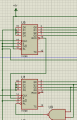
I'm trying to reset this counter when it reaches 6, meaning that I'll get 59 as the last number, but with this circuit, it resets when it reaches 39, and I cannot understand how. NAND gate doesn't even change its state, but the counter resets. When I remove NAND gate, it works fine, but it goes to 99, which is not desirable.
Here's the picture of that part of the circuit.
 

Attachments

WBahn

Joined Mar 31, 2012
32,823
How do you know that the NAND gate doesn't change state? Since you are using an asynchronous load, the pulse out of the NAND gate would be very short.

The problem you are having is very simple: you are using asynchronous logic and have a critical race that you happen to be losing.

Consider the chain of output changes as the counter counts upward, keeping in mind that two signals virtually never change at the same time. So any time more than one output signal changes, the actual transition path could follow any of the possible one-signal-at-a-time paths:

0000 -> 0001

0001 -> 0000 -> 0010
0001 -> 0011 -> 0010

0010 -> 0011

0011 -> 0010 -> 0000 -> 0100
0011 -> 0010 -> 0110 -> 0100
0011 -> 0001 -> 0000 -> 0100
0011 -> 0001 -> 0101 -> 0100
0011 -> 0111 -> 0110 -> 0100
0011 -> 0111 -> 0101 -> 0100

So as your counter goes from 3 to 4, half of the possible paths produce outputs that will cause the NAND gate to go LO, thus resetting the counter.

The part is guaranteed to recognize a load pulse as short as 35 ns, which means that in reality it will actually recognize much shorter pulses, probably less than 10 ns.

Stacking the odds against you is the fact that output changes from HI to LO are considerably longer than changes from LO to HI, thus you are highly likely to follow one of the last two paths as you go from 3 to 4.

This illustrates why people should never implement asynchronous logic designs unless they are willing and able to do the much more detailed design and analysis that is required to avoid just this situation.
 

WBahn

Joined Mar 31, 2012
32,823
If you include the checking of Q0 of U1 then it should work.

Allen
Same problem. There are still two paths in which the outputs will go through the 0110 state when transitioning from 3 to 4. Because the delay is so much higher for H->L transitions than from L-H transitions, you can expect it to take one of the final two paths shown, one of which will glitch the NAND gate. The difference between those is the race between whether Q0 will go LO first, or Q1. That's a coin toss.

It's a bad design.

Even if he gets lucky and it works today, it might not work tomorrow when the chip is at a different temperature or after he's changed the routing of the wires just a bit or puts in a different chip even from the same die.
 

Analog Ground

Joined Apr 24, 2019
460
This is a tricky one. There is a minimum time the LOAD input needs to be low to meet the timing specification. It is a problem to meet this minimum width by simply decoding the outputs. The time it takes for the outputs to change during the load can easily be shorter than the minimum load width, even with the NAND gate delay. The LOAD signal needs a flip-flop to make the LOAD signal synchronous to the "clock" of the U1. There are probably several ways to do this depending on the "clocking" of U1 (using RCO of the other stage or the main clock). I say "clock" because the "clock" of U1 could be the Ripple Clock from U5 and well as the main clock. Both "clocks" can work.
 

WBahn

Joined Mar 31, 2012
32,823
Meeting the minimum LOAD pulse width isn't the problem. When the outputs go to the target state, they will stay in that state until either the next clock event or until the decoded LO on the load line is recognized, assuming the clock isn't running too fast. Since the minimum LOAD pulse width is shorter than the minimum clock period, this shouldn't be the case and thus LOAD pulse will not go away until it has been recognized and acted upon.

The problem is that the LOAD pulse can glitch and be recognized as a valid LOAD pulse during transitions that shouldn't produce a LOAD pulse (which is almost certainly what is happening in this case).
 

Analog Ground

Joined Apr 24, 2019
460
Meeting the minimum LOAD pulse width isn't the problem. When the outputs go to the target state, they will stay in that state until either the next clock event or until the decoded LO on the load line is recognized, assuming the clock isn't running too fast. Since the minimum LOAD pulse width is shorter than the minimum clock period, this shouldn't be the case and thus LOAD pulse will not go away until it has been recognized and acted upon.

The problem is that the LOAD pulse can glitch and be recognized as a valid LOAD pulse during transitions that shouldn't produce a LOAD pulse (which is almost certainly what is happening in this case).
Then, I have to ask, why is there a minimum load pulse width specification? The first output to change, after LOAD starts, will end the load pulse independent of the state of the other outputs. Nothing to do with the clock. Since there is no minimum time from LOAD to an output change, a fully completed load of all outputs cannot be guaranteed. It is a timing violation.

I certainly agree with the possibility of a glitch on LOAD. I think there are two problems. Both of which are solved by making LOAD synchronous to CLOCK.

Edit: I should add I am not claiming the timing violation of my posts is the cause of the TS's original problem. That problem is already solved by WBahn. I am pointing out another problem with the circuit.
 
Last edited:

WBahn

Joined Mar 31, 2012
32,823
Then, I have to ask, why is there a minimum load pulse width specification? The first output to change, after LOAD starts, will end the load pulse independent of the state of the other outputs. Nothing to do with the clock. Since there is no minimum time from LOAD to an output change, a fully completed load of all outputs cannot be guaranteed. It is a timing violation.

I certainly agree with the possibility of a glitch on LOAD. I think there are two problems. Both of which are solved by making LOAD synchronous to CLOCK.

Edit: I should add I am not claiming the timing violation of my posts is the cause of the TS's original problem. That problem is already solved by WBahn. I am pointing out another problem with the circuit.
Two different issues. The minimum load pulse width spec is what the manufacturer is saying WILL be recognized and acted upon properly. They are NOT saying that shorter pulses will not be. The actual minimum pulse width that will be recognized is generally significantly shorter.

The point you make though is technically correct, but very unlikely to happen. By the time the LOAD signal is asserted long enough for the change to be propagated to the first responding output and then through the decoding logic and then to the LOAD input to relax it, it is almost inconceivable that it has not been asserted long enough for all of the other registers to recognize it. But, I will definitely not argue with the claim that this concern is yet another argument against using asynchronous logic in the design of these types of circuits.
 

Analog Ground

Joined Apr 24, 2019
460
At this point the student should see some of the potential problems of using asynchronous parts. Given a choice for this application, a fully synchronous part such as a 74163 decade counter is a better choice. One final caution. Even in a part which is called synchronous, there can be individual functions in the part which are asynchronous. Look into the details. There are a number of traps like this in the 74 series parts.
 
Top