 Facebook
 Google
 GitHub
 Linkedin
Dear Team,
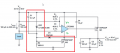
I am going through this article from AD .

I have some questions about this circuit.
1)May I know how the Vout Equation is derived
2)May I know the use of M1 and M2
3)May I know the use of REF and D1
4)Why the GND pin of Opamp is lifted uisng M2
I am going through this article from AD .
I have some questions about this circuit.
1)May I know how the Vout Equation is derived
2)May I know the use of M1 and M2
3)May I know the use of REF and D1
4)Why the GND pin of Opamp is lifted uisng M2

")


