Power amplifier

Thread Starter

jaschek

Joined Sep 5, 2008
7
I am trying to complete a design started by my RF engineer.

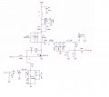
his power amplifier was something like the attachment, power of 500mW and working at a battery voltage of 7.2 V 2100 mAh

can someone help me complete it ??


thanks a ton.
 

Attachments

Thread Starter

jaschek

Joined Sep 5, 2008
7
"Something like" the circuit shown is kinda vague. Can you post up the circuit you are working on?
I said something because some components have not been identified yet, i am sorry the sentence misguides, that is precisely the circuit i am working on...
 

Thread Starter

jaschek

Joined Sep 5, 2008
7
the circuit is supposed to be working at 13.56 mHz. this is for an rfid application.

also the I need to know what values should c11, c12, c50 and L1 have.

thanks beenthere,
 

SgtWookie

Joined Jul 17, 2007
22,230
I can't imagine how this thread will wind up with a happy ending the way things are going.

We don't know where you live, Jaschek - you need to at least put your country in your profile.

In most countries, transmissions on various frequency bands are tightly controlled. Even if you accidentally transmit on a frequency that is not approved for amateur use, you may be subjected to terrible consequences; jail; equipment confiscation; heavy fines; criminal record.

It's up to you to at least tell us where you are via your profile,so that we might help guide you from making terrible mistakes that could result in severe consequenses.

I'm not kidding. Not one bit.
 

Thread Starter

jaschek

Joined Sep 5, 2008
7
Sgt. Wookie

I am sorry i didn't realize the consequences or probably I thought a 500mW transmitter would do no harm especially because I am working with ISO standard proximity cards(13.56MHz).

guess I was wrong, I am from India btw.

thanks
 

beenthere

Joined Apr 20, 2004
15,819
Well, the circuit looks to be almost a joke. How any RF can get past L5, C20-22 and L6 is a mystery. The center pin of the RCA connector is shown grounded, not to an antenna. What is the spec for Q3? What does 680 E have to do with R29? Is R27 really 2 ohms? If Q6 is meant to place Q3 in a proper condition to transmit, what is the function of the network between R25 and R19? Is Q3 supposed to run class C?

The tank in the drain of Q3 (where are Q's 1, 2, and 4 - 7?) would be resonant at 13.56 Mhz if C11 & 12 were 1500pF. C50 provides negative feedback to the gate of Q3, but without knowing Vcc (Vbatt is 7.2 volts, but Vcc is not given) it's hard to guess at a reasonable value for the cap.

Besides, the big filter section between C17 and the RCA jack should attenuate 13.56 MHz by many dB. I would look online for a better circuit.
 

Thread Starter

jaschek

Joined Sep 5, 2008
7
thanks beenthere.

the circuits a joke ?? But I guess i will have to live with the joke for some time !!

*The pin Tx ON is supposed to keep the mosfet from working when not required ( to prevent battery drain), i suppose the network around that pin is for that very purpose.

*I have only produced a part of the schematic here, that should explain the missing transistors.

*Vcc is 5V.

Any more suggestions ??

Q3 - IR LL110
 

beenthere

Joined Apr 20, 2004
15,819
The T filter section following C17 is a problem. At 13.56 MHz, L5 will have an impedance of 58 ohms, L6 will be 85 ohms, and the three parallel capacitors (C20 - 22) will have an impedance of .04 ohms. There won't be any RF left to reach the antenna connector. It looks like a filter to prevent any signal from getting out.

You might consider some solutions already on the market. Texas Instrument has the whole device available - http://focus.ti.com/docs/prod/folders/print/trf7960.html. Get the associated PDF to see what it offers.
 

Thread Starter

jaschek

Joined Sep 5, 2008
7
beenthere,

thanks for being there ;P,

I cannot go ahead with a new design/ product. Suggestions on this circuit/joke would be of great help!!
 
Top