 Facebook
 Google
 GitHub
 Linkedin
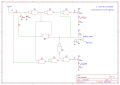
Hi, I am new to electronics and I like you to have a look at the circuit that I've designed as I needed a portable alarm that is actuated by NC contact (break wire, reed switch etc.). This circuit consumes 2uA current in the stand by mode and it can be operated by 9V battery for a long time. It's based on CD4011BE or CD4093BE NAND gate logic. Please suggest any improvement that could enhance the reliability or let me know if there is any mistake in this design.
This is how it works:
1. When the switch is closed, R1 charges the capacitor C1, and inputs of U1.1 remains low since capacitor acting like a short to ground at first. This makes the output of U2.1 low, which means the input 1 of U3.1 is also low. The input 2 of U3.1 is grounded via the break wire and overall this makes the output of U3.1 high, hence the PNP transistor Q2 remains non-conducting and the red led is off. In the same time, if the beak wire connected properly, both inputs of U5.1 are high which means the output is low, thus the green led is on and remains so while the capacitor is charging. This gives the exit delay.
2. When the capacitor C1 is fully charged, the inputs of U1.1 becomes high, which means input 1 of U3.1 is high also. The input 2 of U3.1 becomes high by resistor R4 (3.3M) when the break wire is cut by an intruder, thus the output of this gate becomes low which biases the Q2 into conduction and red led or buzzer is activated.
3. The gates U4.1 and U8.1 function as fail safe feature. If during the installation the break wire is not connected properly, after the switch is closed and while the cap C1 is charging, the inputs of U4.1 are no longer grounded, and the output of U5.1 becomes high, thus the green led is off, indicating something is wrong. The output of U8.1 becomes low for the same reason. This activates Q1 and since the transistor is located after R1, prevents the C1 from charging as current flows directly to ground from emitter- collector path of Q1. This means alarm can never be activated until the contacts are fixed.
I'd appreciate any suggestion to improve the design. Thank you
Attachments
-
 67.8 KB Views: 41
 The 'EMI liability' of the CD4000 series is nothing short of 'legendary'!


