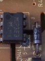
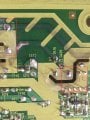
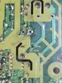
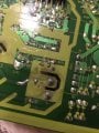
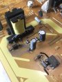
Need to purchase this diode to repair my Panasonic Plasma TV PSU. T2D76 is written on its body and it has a red band on one side. Tried to Google/Digi-key...etc but to no avail. Can anyone help?
Attachments
-
221.9 KB Views: 44
That IC doesn't look so good either.It's probably a Fast Recovery Diode like the BY500 /800 series..
https://www.rapidonline.com/Diotec-...MI_eC_w5HH5AIVgbTtCh0IFQiJEAQYAiABEgL_EvD_BwE
That is probably a flyback SMPS controller. Those DIP-8 packages with one leg missing are quite typical for those. It seems good to me.That IC doesn't look so good either.
kv
I think you meant pin 7 is cut, I was referring to the toasted terminal 8, it looked in line with the suspected diode, seems like I could see some scorched marks on the board leading to the negative on the electrolytic cap also. Something I wouldn't overlook and just replace or at least check.
You looking for cold solder joint, I would call it the black blobIt does look a bit like the joint overheated and the solder balled up (whats the term for that?).
Its PIN 5 tho not pin 8. Pin 6 is the one cut off.
View attachment 186016
Edit: Just noticed its already labeled on silkscreen.
Didn't say it was bad, I just said looks like it took some heat. If he's able to get it up and going then cleans things up, re-soldering all surrounding heated components. If I was in this far, why not change them out? the labor going back in costs more than the components.It doesn't look like solder, but some kind of sealant, IMHO. Normally, then these chips go bad, the "lid" pops off. They literally split in two with a bang.
Kind regards, Samuel Lourenço
I'm right see post #8I think you meant pin 7 is cut, I was referring to the toasted terminal 8, it looked in line with the suspected diode, seems like I could see some scorched marks on the board leading to the negative on the electrolytic cap also. Something I wouldn't overlook and just replace or at least check.
kv
Good Grief, Dave. How long did it take for you to make it back here, you must be all over the forum. I already said I didn't have the correct pin, Post #11 @narkeleptk corrected me.I'm right see post #8
Have you done any rework? Looks better to me now. Still some of them look like they got pretty hot.Have taken closer pictures of the IC and the back of the pcb. These might help.
I see the wicking now that we have better pics. Seen the eyelets.I think that what you are calling scorch marks are just dirt. It looks like this TV comes from a house of smokers. The electrostatic forces near high voltage points will attract dirt and smoke and deposit them on the board. Also, the IC has two eyelets inserted in the board - those are the two circles under the IC. Eyelets allow the solder to wick up the leg more easily, thus you sometimes see the solder balls.
So far, I’ve just taken out D411 and C492 to check out-of-ckt. I don’t have the replacement yet.Have you done any rework? Looks better to me now. Still some of them look like they got pretty hot.
kv
by Robert Keim
by Aaron Carman
by Jake Hertz
by Jake Hertz