PIC16F877A EMI and Noise protection

Please help me check my diagram for any correction? having problem with EMI and Noise

  • N/A

    Votes: 2 50.0%
  • N/A

    Votes: 2 50.0%

  • Total voters
    4

Thread Starter

TalkAboutCircuit

Joined Apr 6, 2015
8
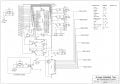
PORT RA0 = 0 and goes high once push button is pressed to extend the cylinder. the problem is sometimes cylinder extend without pressing the push button. Please help me im just a begineer.


Thanks,
 

joeyd999

Joined Jun 6, 2011
5,287
Without a schematic or code, I'd have to use my crystal ball.

And that's at the shop today for repair.

But I did vote "N/A" in your poll.
 

R!f@@

Joined Apr 2, 2009
9,918
And I lost my Crystal Ball. So I dunno anything....!

Still I had to ask where is this push button you are talking about. Can you point it out.
 

blueroomelectronics

Joined Jul 22, 2007
1,757
Wow, what a strange design. What's it supposed to do? Why use the 4017 instead of the extra I/O ports? Why use an ancient 16F877A instead of a 16F887 or 18F4620? Why the opto isolated 7805? Why relays everywhere? Who designed this?
 

joeyd999

Joined Jun 6, 2011
5,287
sorry im new here. and i dont know what should i put in my poll. i uploaded my schematic.
Thanks. Am I correct in assuming CON1 is a break-out connector to which your switch is attached? And the switch connects pin 17 to 16 when pressed?

And tell me the history of R2 and C7, and their purpose.

FYI, you've not posted code. Should I just assume your problem is noise/emi related and not code related?
 

joeyd999

Joined Jun 6, 2011
5,287
Try this network (and eliminate R2 and C7). It eats just about any noise you can throw at it, and protects the MCU at the same time.

Route "DIGIN0" to RA0, and the switch between pin 17 and ground. You'll have to add a ground to one of your free pins on CON1, as you don't seem to have one.

The circuit *will not* alleviate the need for software debouncing, if you haven't done it.


Thread Starter

TalkAboutCircuit

Joined Apr 6, 2015
8
Hi joey, your right for the CON1. R2 and C7 is my pulldown resistor and filter. i put this thinking that it will solve the issue for the noise problem.\

For the code. i used flowcode V5? should i post it?

ok will give you feedback if it works.

Hi R!f, DB25 pin 16 and 17 is connected to the push button.
 
Last edited by a moderator:

Thread Starter

TalkAboutCircuit

Joined Apr 6, 2015
8
Try this network (and eliminate R2 and C7). It eats just about any noise you can throw at it, and protects the MCU at the same time.

Route "DIGIN0" to RA0, and the switch between pin 17 and ground. You'll have to add a ground to one of your free pins on CON1, as you don't seem to have one.

The circuit *will not* alleviate the need for software debouncing, if you haven't done it.


Would it solve the problem if i put a debouncing in my software?IF yes?should i still eliminate R2 and C7?
 

joeyd999

Joined Jun 6, 2011
5,287
Would it solve the problem if i put a debouncing in my software?IF yes?should i still eliminate R2 and C7?
You will continue to require R2 as the pullup (if you don't use the proffered network). I don't like putting caps on inputs -- I prefer sharp edges.

You should *always* debounce mechanical inputs, either through hardware or software. Software is easier and more reliable.

I don't know if your flowcode package incorporates debouncing for you, but, yes, if it doesn't, you should add it.
 

Thread Starter

TalkAboutCircuit

Joined Apr 6, 2015
8
Yes my flowcode have debouncing on it.but no idea how long the interval im gonna use. and for the R2?should i use it as a pullup?or a pulldown?
 

joeyd999

Joined Jun 6, 2011
5,287
Yes my flowcode have debouncing on it.but no idea how long the interval im gonna use. and for the R2?should i use it as a pullup?or a pulldown?
Normally, I treat mechanical switches as "active low," meaning they pull an input to ground. This way I don't need my PCB's Vdd flying out into space risking shorts. In this case, I'd use a pullup resistor (or, the weak pullups incorporated into some of the MCU pins).

You designed for "active high", which means you need pulldown resistors.

The network I showed you is active low from the point of view of the switch, *but* there is an inversion through the 2222. Therefore, the MCU input will see it as active high. No code changes will be necessary.

BTW, I prefer to call the network a "contact-closure" input. I'd usually have two pins on my break-out connector for each switch. One, naturally, would be tied to ground on the PCB, and the other to the input of the network. To activate, it is only necessary to cross the two wires -- i.e. close the contact. This prevents the possibility of inadvertently creating a ground-loop. In your case, if you had multiple switch inputs, you'd need to snake a ground (or, wrt your schematic, +5V) to lots of different places. This is asking for trouble down the road.
 

joeyd999

Joined Jun 6, 2011
5,287
Also, the network provides two additional advantages:

1. The open circuit voltage (the voltage across the switch contacts) never exceeds 0.7V.
2. The short circuit current (the current through the closed switch, or an inadvertent short to ground) never exceeds 500uA.

This is sometimes important for safety or certification reasons.
 

Thread Starter

TalkAboutCircuit

Joined Apr 6, 2015
8
30ms is good for debouncing. Also the 16F877A has a weak pull-up option on PORTB. Ideal for pushbuttons. Any reason you're using the CD4017?
ok my project is about multiplexing. where using a one machine
30ms is good for debouncing. Also the 16F877A has a weak pull-up option on PORTB. Ideal for pushbuttons. Any reason you're using the CD4017?
Ok thnx. To bad that i use most of my PORTA as input. and PORTB as output. the problem is that prototype is already running on the production line. CD4017 use as a switching of relay every time it receive signal from the machine. do you want me to explain how may project works?
 

Thread Starter

TalkAboutCircuit

Joined Apr 6, 2015
8
Normally, I treat mechanical switches as "active low," meaning they pull an input to ground. This way I don't need my PCB's Vdd flying out into space risking shorts. In this case, I'd use a pullup resistor (or, the weak pullups incorporated into some of the MCU pins).

You designed for "active high", which means you need pulldown resistors.

The network I showed you is active low from the point of view of the switch, *but* there is an inversion through the 2222. Therefore, the MCU input will see it as active high. No code changes will be necessary.

BTW, I prefer to call the network a "contact-closure" input. I'd usually have two pins on my break-out connector for each switch. One, naturally, would be tied to ground on the PCB, and the other to the input of the network. To activate, it is only necessary to cross the two wires -- i.e. close the contact. This prevents the possibility of inadvertently creating a ground-loop. In your case, if you had multiple switch inputs, you'd need to snake a ground (or, wrt your schematic, +5V) to lots of different places. This is asking for trouble down the road.

Ok. i think i need to reconstruct my schematic and implement what i learn today. i still have a long way to go.
 
Top