Facebook
 Google
 GitHub
 Linkedin
Hi everyone,
I’ve just finished routing my very first two-layer PCB and would love a second (or third!) set of eyes before I order boards.
Project at-a-glance
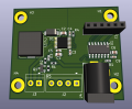
Schematics (PDF) and layout screenshots are attached.
Key layout decisions
Specific questions for reviewers
Thanks a ton for taking the time to look - your feedback will make this board (and my next one) much better.
I’ve just finished routing my very first two-layer PCB and would love a second (or third!) set of eyes before I order boards.
Project at-a-glance
| Function | Device | Notes |
|---|---|---|
| Boost LED driver | Linear LT3478 | Drives a single 10.9 W white LED at 1000 mA (VIN = 5 V → VLED ≈ 12 V) |
| Logic-level translator | TI 74AHCT125 | Converts 4 V3 MCU signals to 5 V for an external APA102 strip |
| Supply rails | 5 V input, 3 V3 logic | 3V3 generated off-board |
Schematics (PDF) and layout screenshots are attached.
Key layout decisions
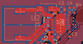
- Ground strategy — split planes
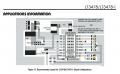
- The LT3478 datasheet recommends an “analog GND” return for RT and VC (exposed pad, Pin 9) that is separate from the switch/power GND at Pin 16 (see attached datasheet Figure and annotated layout).
- I implemented this by pouring two copper zones on the top layer:
- AGND surrounding Pin 9 (RT/VC network)
- PGND surrounding Pin 16 (switching loop)
- In the attached layout I indicated the split between both copper zones in yellow. AGND and PGND meet under the IC.
- Hot-loop minimisation
- Switch node → inductor → Schottky → Cin traces kept as short and wide as possible (max loop area ≈ 180 mm²).
- 1 oz copper with 1 mm (39 mil) traces on this loop to tolerate >1 A peak.
- Thermal & noise considerations
- Filled copper beneath the inductor for heat-spreading and to lower impedance.
- Level-shifter rail filtered with ferrite bead + 10 µF + 0.1 µF right at the 74AHCT125 VCC pin.
Specific questions for reviewers
- AGND vs PGND implementation
- Does the split-plane approach satisfy the datasheet’s intent? On paper it matches the recommended example, yet I’d appreciate confirmation.
- Decoupling & filtering
- Placement of the 74AHCT125 ferrite/caps looks acceptable?
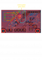
- Thermal vias
- I used 0.3 mm drills, 0.6 mm OD, 6 vias under the LT3478 paddle. Is that adequate for a 10 W load?
- Anything else
- Silkscreen clarity, manufacturability quirks, rule-of-thumb violations, feel free to be brutal. I’d rather hear it now than after I fry LED #1!
Thanks a ton for taking the time to look - your feedback will make this board (and my next one) much better.
Attachments
-
 277.7 KB Views: 3
 -
 223.6 KB Views: 3
 -
 261.3 KB Views: 3
 -
 328.6 KB Views: 3
 -
127.7 KB Views: 1
-
288.3 KB Views: 0