 Facebook
 Google
 GitHub
 Linkedin
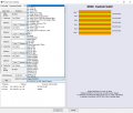
How do we select the dielectric material to be used in the PCB stackup. The list is long, see attachment. How we can do price wise comparison.
I just have a look at some typical stackups for standard PCBs. They have used 18 um (0,5 oz) on outer layers and 35 um (1 oz). Any reason for thinner copper layers on top and bottom. I guess a 10 mil trace can carry more current in inner thick layers compared to outer thin layers. Is that correct ?
Regarding the dielectric, we are working with standard PCB with typical heights 1.6 mm or 2.4 mm which are not flex PCBs.
In the picture I shared, there are many FR4 dielectric in the list. What is the difference between high Tg, low Tg and mid Tg ? What is low CTEz and inorganic filters ? I would like to understand the consequences of these parameters while selecting the FR4.
Rogers is a name of the company or dielectric material ?
There is list of Rogers dielectric in the picture. Which one is better for high speed signals for example 10 Gbps Ethernet, USB 3.0 and PCI 3.0 in the design.
Attachments
-
 51.2 KB Views: 3


