 Facebook
 Google
 GitHub
 Linkedin
Hello,
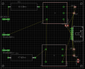
i am really confused about how to routing the circuit in the picture. The squares T1 and T2 are voltage transducer LV 25-p and at the clamp J3 are about 700V and at clamp J1 there are about 490V. I dont understand how to route this circuit without getting in trouble with creepage and clearance. I would be thankful if someone could help me with this topic.
i am really confused about how to routing the circuit in the picture. The squares T1 and T2 are voltage transducer LV 25-p and at the clamp J3 are about 700V and at clamp J1 there are about 490V. I dont understand how to route this circuit without getting in trouble with creepage and clearance. I would be thankful if someone could help me with this topic.
Attachments
-
 36.8 KB Views: 6


