Facebook
 Google
 GitHub
 Linkedin
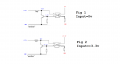
Let us analyse this design together, I have several points to clarify with you so I will make a bulleted list.
Tell me if I am wrong.
1) On the left, if I'm not mistaken, Vdd takes on the value of Va or Vb depending on which is present, right? So it is as if they are in OR?
If both Va and Vb are ON ... Vcc is equal to the higher value of the two?
Now let's focus on the right side.
Let's assume that DCX_OK and DCY_OK are "status" signals, i.e. they tell me whether +3.3_X and +3.3V_Y are good or not (whether they work or not)
2) The central bjts (BJT1 and BJT2) will be closed or opened depending on whether +3.3_X and +3.3V_Y on their base are present or not, right?
3) If +3.3_X is present, that opto-bjt1 (suggest name) will close and then C and B of BJT1 will short? I don't quite understand how OBJT1 works ... of
4) If the answer is yes, how does BJT1 close when C=B? .. usually closure implies that E and C are ideally a "wire"

Please, if possible, answer in order, perhaps respecting the bulleted list
Thanks
Tell me if I am wrong.
1) On the left, if I'm not mistaken, Vdd takes on the value of Va or Vb depending on which is present, right? So it is as if they are in OR?
If both Va and Vb are ON ... Vcc is equal to the higher value of the two?
Now let's focus on the right side.
Let's assume that DCX_OK and DCY_OK are "status" signals, i.e. they tell me whether +3.3_X and +3.3V_Y are good or not (whether they work or not)
2) The central bjts (BJT1 and BJT2) will be closed or opened depending on whether +3.3_X and +3.3V_Y on their base are present or not, right?
3) If +3.3_X is present, that opto-bjt1 (suggest name) will close and then C and B of BJT1 will short? I don't quite understand how OBJT1 works ... of
4) If the answer is yes, how does BJT1 close when C=B? .. usually closure implies that E and C are ideally a "wire"
Please, if possible, answer in order, perhaps respecting the bulleted list
Thanks