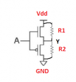
With Vin = 0V, you've indicated that the NMOS is off. So remove it from the circuit. Now also remove the bottom resistor. This leaves you with the PMOS and a pullup resistor. Can you figure out what Vout is? Again, assume that the resistor is sized such that it only lightly loads the transistor.
Id = k (Vsg - Vt)^2 = k (Vout - Vin - Vt)^2
With Vin = 0V, Id = k (Vout - Vt)^2
Vout = Vdd - Id*R1 = Vdd - k*R1 *(Vout - Vt)^2
Solving for Vout, I get:
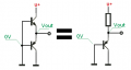
I don't know why the two circuits are equivalent. However, for the circuit on the left, Vout = 0.7V with the assumption that Vbe is constant and equal to 0.7V.
BTW, why can we replace the npn transistor by a resistor?
Shouldn't the transistor be OFF? So, it is open circuited. As a result, there is no current flowing through the pnp transistor and the pnp is also OFF. That is my confusion.
Because we always have some small leaking current. And this resistor help as visualizes this current. So we the P-MOS we have Vout = Vin + Vgs and for Vin = 0V ---->Vout = Vgs. Because Id current is very small and this is why Vgs = Vp
\(Vgs = (1 - \sqrt{\frac{Id}{K}}) * Vp\) so for Id = 0A Vgs = Vp.
I think this is sub-threshold operating region. I have been reading about it for some time but doesn't get a good grasp of it.
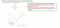
For the input-output characteristic of the buffer, I think it is not completely exact.
As Vin = 0, Vout = Vt as you said above.
However, as 0< Vin<Vt, Vout = Vin + Vt not just Vt.
Am I right?
I think this is sub-threshold operating region. I have been reading about it for some time but doesn't get a good grasp of it.
For the input-output characteristic of the buffer, I think it is not completely exact.
As Vin = 0, Vout = Vt as you said above.
However, as 0< Vin<Vt, Vout = Vin + Vt not just Vt.
Am I right?
But if Vout = Vt when Vin = Vt, then that means that the Vgs of the PFET is 0V, in which even a high resistance (such as an NFET with just a little bit of leakage) will pull the output node up toward the upper rail. This will continue until the Vgs of the PFET reaches about a threshold voltage at which time the PFET will turn on just enough to hold that voltage.
What you will find instead of the diagram given in the answer, is that there will be a deadband in the middle that is about the width of the sum of the two threshold voltages. If you think about it, if the voltage is at half the supply voltage, then the system is basically symmetric (assuming balanced transistors) and there is no reason for the output voltage to be anything other than half the supply voltage. That situation won't change appreciably until the input voltage either moves upward by an NFET threshold voltage or downward by a PFET threshold voltage.

 Facebook
 Google
 GitHub
 Linkedin

 129.4 KB Views: 29