 Facebook
 Google
 GitHub
 Linkedin
Hi everyone!
I am currently developing a prototype for a device based on an Arduino Due. My background is in computer sciences, so my knowledge on electronics is quite limited. And currently I am facing a blocking problem in this development.
I have designed and printed a PCB that includes a stereo analog amplifier (LM4808) and a MicroSD Shield mounted on top of an Arduino Due board (the schematic for the amplifier circuit part of the PCB is attached). The idea is to be able to play WAV files from a MicroSD card. After I finally assembled the amp and SD shield in the PCB, I tested the sound and found that there was a significant amount of noise.
First I checked for software issues, and I can assure that it's not a problem, as the whole playing procedure is adapted from a previous version working with an Arduino Zero and a LM386 amplifier (mono).
I also checked generating a sinusoidal wave (thus not using the SD card): the noise disappears and the oscilloscope shows a perfectly well synchronised wave at the various testing frequencies.
The problem arises when I do use the SD card. I suspect that it's some kind of isolation problem between the digital circuit (SPI for SD card reader) and the analog circuit (amp). When I touch with my hand the CLK (clock) signal of the SPI bus, the noise is somehow modulated. In a non-pcb version that I tested before printing, when the SPI wires were close to the AMP, there was more noise. In a previous design (Arduino Zero and LM386), this noise disappeared when I printed the PCB, but it's not the case in this situation.
I am currently out of clues on how to proceed. My fear is that I will continue to print different PCBs with no significant changes to try to isolate this noise by changing the routing, positions and adding ground planes. Can someone suggest me the proper way to proceed in this case?
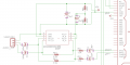
I am attaching the parts of the schematic related to the amplifier, the part of the eagle board design and an image on the circuits mounted on the PCB. The PCB includes several other components, but there are mostly TTL lines to control input and output. Currently, no other component is mounted on the PCB but the ones in the image.
Any help will be greatly appreciated.
Thanks!


I am currently developing a prototype for a device based on an Arduino Due. My background is in computer sciences, so my knowledge on electronics is quite limited. And currently I am facing a blocking problem in this development.
I have designed and printed a PCB that includes a stereo analog amplifier (LM4808) and a MicroSD Shield mounted on top of an Arduino Due board (the schematic for the amplifier circuit part of the PCB is attached). The idea is to be able to play WAV files from a MicroSD card. After I finally assembled the amp and SD shield in the PCB, I tested the sound and found that there was a significant amount of noise.
First I checked for software issues, and I can assure that it's not a problem, as the whole playing procedure is adapted from a previous version working with an Arduino Zero and a LM386 amplifier (mono).
I also checked generating a sinusoidal wave (thus not using the SD card): the noise disappears and the oscilloscope shows a perfectly well synchronised wave at the various testing frequencies.
The problem arises when I do use the SD card. I suspect that it's some kind of isolation problem between the digital circuit (SPI for SD card reader) and the analog circuit (amp). When I touch with my hand the CLK (clock) signal of the SPI bus, the noise is somehow modulated. In a non-pcb version that I tested before printing, when the SPI wires were close to the AMP, there was more noise. In a previous design (Arduino Zero and LM386), this noise disappeared when I printed the PCB, but it's not the case in this situation.
I am currently out of clues on how to proceed. My fear is that I will continue to print different PCBs with no significant changes to try to isolate this noise by changing the routing, positions and adding ground planes. Can someone suggest me the proper way to proceed in this case?
I am attaching the parts of the schematic related to the amplifier, the part of the eagle board design and an image on the circuits mounted on the PCB. The PCB includes several other components, but there are mostly TTL lines to control input and output. Currently, no other component is mounted on the PCB but the ones in the image.
Any help will be greatly appreciated.
Thanks!
Attachments
-
 90.2 KB Views: 2


