 Facebook
 Google
 GitHub
 Linkedin
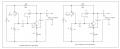
My revisions of a published design of a pink noise generator are as follows:
1. Vcc reduced from 18V to 15V
2. transistors Q1 and Q2, PN2222A substituted for 2N2712
3. Bias resistor R3 increased from 1 Meg-Ohm to 10 Meg-Ohm
The substituted transistors are what I have on hand. Resistance of R3 was increased to increase measured collector voltage of Q2 with respect to ground (after making the first two revisions) from about 1.5V to 7.5V.
Is the revised circuit still a legitimate pink noise generator, or are my revisions in error? Measuring with a DMM that reads AC voltage accurately to 1 kHz, the audio output level reads 48 mV which I would think is too low. Is this about the voltage output level that the circuit should produce?
Thanks in advance for your comments,
Pete
Attachments
-
 5.8 KB Views: 4


")


