Next Report - Application circuits for BJTs

ericgibbs

Joined Jan 29, 2010
21,569
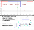
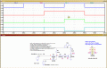
One way is to have 2, voltage sources ,set for pulse operation.

By setting the the pulse start delay and the tOn and tPeriod times for each source you can simulate the 'AND' gating pattern you have posted.

You also set the On voltage level and Off voltage levels.

Do you follow OK.?
 
Last edited:

ericgibbs

Joined Jan 29, 2010
21,569
This is my method, I expect you do not have the Dview models.??

If not get them from the Yahoo LTS User group, you will find them very useful for digital sims.
 

Attachments

Thread Starter

PsySc0rpi0n

Joined Mar 4, 2014
1,786
This is my method, I expect you do not have the Dview models.??

If not get them from the Yahoo LTS User group, you will find them very useful for digital sims.
Ok, thanks for the info. I think I'm not going to complicate it more for now... I'm going to leave it as it is for now!

I need one more help...

Our teacher is asking what is the importance of the diode D3. Can you give me a help? I think it might have something to do with the Vbe voltage drop and the need of compensation to keep diodes at "ON" state. But I'm not quite sure and how to explain it!
 

ericgibbs

Joined Jan 29, 2010
21,569
Consider that the Vbe drop across a forward biased diode is say 0.7V and you already know that a transistor can be brought into conduction with a Vbe of 0.61V.

From this, you should be able to figure out the purpose of that D3 diode, what do you think it is.??
 

Thread Starter

PsySc0rpi0n

Joined Mar 4, 2014
1,786
I don't know if I understood your point. If the D3 is forward biased, it will go thru it around 0.7V that will ensure that there will be always at least 0.7V of drop at BE junction and that that will also ensure that the BJT is always as it's active zone??? Is that it?
 

ericgibbs

Joined Jan 29, 2010
21,569
I don't know if I understood your point. If the D3 is forward biased, it will go thru it around 0.7V that will ensure that there will be always at least 0.7V of drop at BE junction and that that will also ensure that the BJT is always as it's active zone??? Is that it?
Condition #1:
Assume St1 & 2 are Low say at 0V, the junction of D3 and R1 will be at ~0.7V. and the transistor will be Off, not conducting.

To turn On the transistor the voltage at the junction of D3 and R1 would have to be the sum of the forward drop of D3 and the transistor Vbe, say 0.7V + 0.65V.

Condition #2:
When both St1 and 2 are BOTH high at say 5V, the voltage at the junction of D3 and R1 will be pulled up by the 2K2, to a voltage that will exceed 0.7V+0.65Vbe and the transistor will be switched On,,, Vcol will be pulled down to near zero volts.

In practice in Condition #1, its possible for the St1 and 2 not to be at 0V, but some higher voltage say upto 1V, this would not hold the junction of D3 and R1 at 0.7V, but at 1.7V. So the transistor, without the D3 diode could turn On.


D3's purpose is to increase the Off threshold Voltage at St1 and 2.

Ok.?
 

Thread Starter

PsySc0rpi0n

Joined Mar 4, 2014
1,786
I will process your explanation later. Now I need to move on to the next circuit, attached!

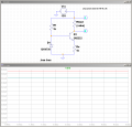
The next circuit, is the attached one. Teacher asks to calculate the current thru R load.


If I use the "input net" equation, Vcc = R_load(I_Vcc - I_R1) + Vce + ReIe (hope it is correct), knowing that Ib = Ic/β and Ie = ((β+1)/β)Ic, how can I calculate I_R1???

We have been using Thevenin's Theorem in some cases but no zeners in those cases and we also have a resistor where we have now the zener! So, I'm not sure If I should use Thevenin here to make the circuit more simple and try to calculate I_R1 from there.

If I try to do it without Thevenin I use the equation above to get my I_R1 but the problem is that I don't know the current thru Vcc that I have called I_Vcc.
 

Attachments

ericgibbs

Joined Jan 29, 2010
21,569
hi,
Why not consider this method.

You know that the zener is 4.7V also Vbe is a nominal 0.7V

So from that you can work out Ve, then Ie.

Knowing Ie and the Beta you can calc Ib, then you calc Ic and then Vc for the different values of Rload.

Note: your model shows the zener is lower than 4.7V so the sim will be a little different from your calculations.
 

Thread Starter

PsySc0rpi0n

Joined Mar 4, 2014
1,786
Ok, I will try to do it that way.

Please, also check if my equations are correct and what would be the zener that would be closer to my calculations? I choose that one because LTSpice has it's Breakdown Voltage = 4.7V.

Vzener - Vbe - Re*Ie = 0, is correct?
 

ericgibbs

Joined Jan 29, 2010
21,569
Ok, I will try to do it that way.

Please, also check if my equations are correct and what would be the zener that would be closer to my calculations? I choose that one because LTSpice has it's Breakdown Voltage = 4.7V.

Vzener - Vbe - Re*Ie = 0, is correct?
Yes,
Zener voltage is as specified on its datasheet.
 

Thread Starter

PsySc0rpi0n

Joined Mar 4, 2014
1,786
Yes,
Zener voltage is as specified on its datasheet.
I'm assuming you said "yes" to the equation being correct.

Then you said that that zener didn't have 4.7V as Breakdown Voltage and that my results wouldn't be as LTSpice would show. So, what should be the zener to pick up so that results are closer to my calculations?

Edited;

You said the with Vzener and Vbe I can get first Ve and then Ie?

I was calculating first Ie then Ve like:

Vzener - Vbe - Re*Ie = 0

4.7 - 0.7 - 1k*Ie = 0 <=> Ie = 4mA

Then Ie*Re = Ve <=> 4V

Then you said after knowing Ie and β I could calculate Ib. How come?
 
Last edited:

Thread Starter

PsySc0rpi0n

Joined Mar 4, 2014
1,786
So Ie = 4mA.
Ie = Ic + Ib
<=> Ie = Ib/β + Ib
<=>Ib = Ie/((1/β)+β)
<=>Ib = 15.58μA

Ic = 15.58*256.7 = 4mA

Is this correct?
 

Thread Starter

PsySc0rpi0n

Joined Mar 4, 2014
1,786
Ok, i was stupid when I replaced Ic by Ib/β.

I got Ic = 3.98mA!

If I change R_load, will Ic also change?

All the calculations I have done so far for Ic, didn't envolved R_load ever!
 
Last edited:
Top