Need this module schematic diagram and BOM

Thread Starter

Anthony-K

Joined Aug 2, 2025
12
that is the choice you need to make yourself. i cannot solve all worlds problem. even if i could, you did not state where you are and what sources you use.

i often use JLC and change designs so that it can work with parts that JLC stocks. that way i can order assembled boards. PCBA does not cost much and parts tend to be a lot cheaper than what i would normally be able to get through main distributors (Mouser, DigiKay, Newark...).

at any rate, all of the parts seem to be ultra low cost anyway. what do you think my time is worth?
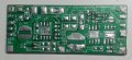
Yes, it was definitely worth it. You helped me a lot by finding that similar design, it has the exact things (Schematic diagram, BOM, and also PCB design) that I wanted. Thanks for your time and help. I appreciate that.
 

Plamen

Joined Mar 29, 2015
111
View attachment 357851
This is a 12V Mini UPS circuit board. I am trying to design it for my project. I need help with it's schematic diagram and BOM. I couldn’t find any datasheet or diagrams for this anywhere. Somebody please help me to design this.
I have reverse engineered several similar UPS modules from Ali. I have created KiCad schematics for them with all parts' values, but a few unmarked ceramic capacitors. Write down the ICs used on the board. Download their datasheets and examine typical application. Compare with your board. On the photos I cannot see the chips marking, but the interconnections are visible.
I can send you several examples, but if you really want to reverse engineer this one - bear in mind it is very time consuming, especially without the real board to buzz with DMM to confirm connections. I see 3 ICs and two inductors. From block diagram stand point, we expect to see a battery charger IC (linear), a boost circuit (to make 12V out of say 3 to 4.2V) and a pair of ideal diodes (most likely based on MOSFETs). The bottom picture is flipped around a vertical axis in respect of the first.
The incoming power has to come to the charger circuit and via ideal diode to the input of the boost circuit (where also via diode should come the battery voltage). There may be protective circuit associated with the battery (limiting current)
 

Thread Starter

Anthony-K

Joined Aug 2, 2025
12
I have reverse engineered several similar UPS modules from Ali. I have created KiCad schematics for them with all parts' values, but a few unmarked ceramic capacitors. Write down the ICs used on the board. Download their datasheets and examine typical application. Compare with your board. On the photos I cannot see the chips marking, but the interconnections are visible.
I can send you several examples, but if you really want to reverse engineer this one - bear in mind it is very time consuming, especially without the real board to buzz with DMM to confirm connections. I see 3 ICs and two inductors. From block diagram stand point, we expect to see a battery charger IC (linear), a boost circuit (to make 12V out of say 3 to 4.2V) and a pair of ideal diodes (most likely based on MOSFETs). The bottom picture is flipped around a vertical axis in respect of the first.
The incoming power has to come to the charger circuit and via ideal diode to the input of the boost circuit (where also via diode should come the battery voltage). There may be protective circuit associated with the battery (limiting current)
Hello Plamen, thanks for your advice, thatbs really helpful. From the board I get this parts U1 = A-l QFMA (I didn't find this chip online), U2 = XR2681, U3 = XB8089D, R1 = T110, L1= 4R7, L2 = 3R3, D1 = SS34. I do have a real board of it. I desoldered the parts for better clear traces. I am trying to reverse engineer it. Trying to find those datasheets the ICs. The main problem I am facing with it's ceramic capacitors hopefully I can reverse engineer this. I need a suggestion that I need to connect 4 18650 lithium batteries. Use a smart safe charging system for those batteries. Get 12v 2A output and it should be work as a mini UPS. If you have any similar designs please feel free to share with me.
 

Attachments

MrAl

Joined Jun 17, 2014
13,707
Stealing a design for your own DIY project is still stealing.
This could fall under the Fair Use Act. It could function as a reference design not a complete hack off. I suspect that is the intent.
Who would care if you made one for yourself only.
 

MrAl

Joined Jun 17, 2014
13,707
View attachment 357851
This is a 12V Mini UPS circuit board. I am trying to design it for my project. I need help with it's schematic diagram and BOM. I couldn’t find any datasheet or diagrams for this anywhere. Somebody please help me to design this.
You mean you want to build one just like it but not exactly the same? That should be ok I would think.
With the right to repair you have to know the circuit, you just can't reproduce it and sell it. If you don't sell it, it's also probably ok but this may vary with your region. You'd have to ask a local lawyer I guess.

As far as the learning experience, I can't see anything wrong with it. If you had the schematic you would learn from it you just don't want to make the same exact thing.

UPS products and switching power supplies are not that easy to build even if you have a schematic, although that does help a lot.
It may be hard to get one to work anyway without constantly blowing transistors.

You could start by looking for designs on the web that are already written with a schematic. You could start with a switching power supply as that is the main component. Get that working first, that's the hardest part.

Maybe you should post your past design experience and members can recommend how to proceed.
 

DickCappels

Joined Aug 21, 2008
10,661
From the product page: "
!!! Be careful. When the UPS operates without a battery, the XR2681 chip may burn out !!!"

Are you sure you want to have a circuit with this problem?
 
Top