Need help tweaking a clap switch based on two 555's and a 4017

Thread Starter

Johnnz

Joined Dec 31, 2008
55
Hi all,
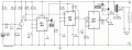
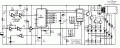
Happy New Year from New Zealand. I'm a first time poster in this forum and hoping to get some (perhaps many- if I have time and you have patience) questions answered about a little circuit I have been building over the last couple of days based on this page: http://www.electronicsforu.com/electronicsforu/lab/ad.asp?url=/EFYLinux/circuit/may2003/ci4-clap.pdf&title=Clap%20Switch .

Basically, things aren't working consistently in my finished build. I know that IC1 is doing its thing since the red led comes for three seconds on first clap, but I can't always get IC2 to produce a signal from its output (when measured for voltage on pin 3 when clapping while the red led is still on). I have swapped the two ics around and they both work in IC1 position (despite one being labeled as LM555CN and the other NE555P - should that matter?)

The circuit will sometimes work, but if I disconnect and reconnect power (9v) only IC1 will be functioning again with the red led lighting up once IC1 provides output.

Also wondering, Does it matter that I have used a Tantalum capacitor 0.68uF rather than 0.1uF recommended for C1, and how should I adjust the sesitivity of the microphone? I have also used 0.033uF ceramic caps rather than 0.01uF for C4 & C5?

It is getting quite frustrating that I cant get consistent operation from this circuit. It does work properly sometimes, then if I try a minute later it wont:confused:

just noticed some other curious behaviour: when it is working properly, there is the odd time that the green led will just momentarily flicker rather than latch on. How is that possible? I thought that IC3 was acting as a flip flop based on the output of IC2 which is also in monostable operation?

I have probably left out some important other info, but I'll post now or else I'll go barmy trying to do it alone!!
 
Last edited:

Wendy

Joined Mar 24, 2008
23,415
C1 will make a little difference. It is basically part of a high pass filter as well as signal conditioner.

The second 555 MUST have a high on pin 4, it is disabled by the first 555 normally. I would measure this voltage.

I covered the 555 monostable in this experiment.

Other improvements is to get a Solid State relay and replace the relay the original design has. Neat circuit though, I now know how a clapper works.


Attachments

Last edited:

Thread Starter

Johnnz

Joined Dec 31, 2008
55
Thanks for that reply. Though I just realise that I meant C2 was the one I used a 0.068 Tantalum for not C1. Any more help and ideas appreciated Thanks.

pin 4 of IC2 is getting 7.08v when IC1 is engaged.

From my calculations IC2 is sending a pulse to IC3 for about one thousandth of a second, so perhaps that is what the green led is flashing for sometimes when IC3 fails to latch into the alternative state?
 

Wendy

Joined Mar 24, 2008
23,415
If the first 555 is triggering the second should be too, since they use the same signal. Like I said, check pin 4 of IC2, it needs to be a high. Since it has a filter cap there is several things that can go wrong there. I believe R10 and C7 could be eliminated with no problem. Looking at it, pin 8 of IC2 should also go to the + power supply. I think they are trying (erroneously in this case) to save juice.

R11 is also not needed. I do believe whoever designed that circuit didn't have a clear idea how a 555 works.

If they really wanted to save juice they would use a CMOS 555 and eliminate the LEDs

********************

It occured to me that the reason they had R11 is because they aren't powering up the IC2. Bad design though, try connecting pin 8 (the power supply pin of the 555) to 9V and see if it doesn't work better. This is also why they have R10 and C7, they are delaying the pulse until the chip is powered up. A 7555 (CMOS 555) would eliminate those parts nicely.

Using the same concept you could add another 555 and make a triple clapper.
 
Last edited:

Thread Starter

Johnnz

Joined Dec 31, 2008
55
If the first 555 is triggering the second should be too, since they use the same signal. Like I said, check pin 4 of IC2, it needs to be a high. Since it has a filter cap there is several things that can go wrong there. I believe R10 and C7 could be eliminated with no problem. Looking at it, pin 8 of IC2 should also go to the + power supply. I think they are trying (erroneously in this case) to save juice.


R11 is also not needed. I do believe whoever designed that circuit didn't have a clear idea how a 555 works.

If they really wanted to save juice they would use a CMOS 555 and eliminate the LEDs

********************

It occured to me that the reason they had R11 is because they aren't powering up the IC2. Bad design though, try connecting pin 8 (the power supply pin of the 555) to 9V and see if it doesn't work better. This is also why they have R10 and C7, they are delaying the pulse until the chip is powered up. A 7555 (CMOS 555) would eliminate those parts nicely.

Using the same concept you could add another 555 and make a triple clapper.
According to the description, R10 and C7 are to prevent IC2 false triggering on first clap (also the reason IC2 is not powered by direct connection to the battery). The second clap should trigger IC2 while it is still powered up by IC1, for about 3 seconds from first clap.
 

Thread Starter

Johnnz

Joined Dec 31, 2008
55
I think that most old circuits on that website in India don't work.
Uh:rolleyes:. I've about given up on it anyway. There's only so much clapping one can do during testing before one is well ready to throw away the idea of having a clap operated anything:mad:
 

Wendy

Joined Mar 24, 2008
23,415
According to the description, R10 and C7 are to prevent IC2 false triggering on first clap (also the reason IC2 is not powered by direct connection to the battery). The second clap should trigger IC2 while it is still powered up by IC1, for about 3 seconds from first clap.
OK, I see your point. But anytime you power a chip up just before using it you're asking for trouble. The delay provided R10 and C7 should be enough. So, are you seeing the high on pin 4? Pin 4 is all you need to prevent false triggering, it is the chip disable pin.

Something a lot of people designing the 555 miss, the high on the 555 is 1.4V less than the power supply line.
 

Wendy

Joined Mar 24, 2008
23,415
Good luck with it, let us know how it works out. To my eye it looks like it would be less reliable, but I've been wrong before.


The advantages of having a power supply tap are good, but I don't think I like the SCRs (ie, AC) and the low power stuff contacting.
 

Attachments

eblc1388

Joined Nov 28, 2008
1,542
Uh:rolleyes:. I've about given up on it anyway. There's only so much clapping one can do during testing before one is well ready to throw away the idea of having a clap operated anything:mad:
Just give the following circuit modification another go to see if it now works.


Good luck to you.
 

Attachments

Thread Starter

Johnnz

Joined Dec 31, 2008
55
Success!!!
I finally had the breakthrough with this little circuit neccessary to getting consistant operation from it. Got back from holiday trip to the beach yesterday and found some time (and patience) this afternoon to do some more troubleshooting...

Basically, all that was wrong with the initial design was that the "enable" pin (pin 13) on IC3 required connection to ground. I only realised this after doing some reading online regarding CMOS ICs always needing their inputs tied to +ve or -ve, (even) if they are not being used.

I did try your suggestion too Chung, but there was no noticable change in operation.

Also learnt that R11 is there so that the clock input of IC3 is not left 'floating' when there is no high signal from IC2 - similarly as above - just giving a better point of reference for the input clock pin.

Just need to make the circuit more clap sensitive now. What components around the condensor microphone should be changed to achieve this?

Thanks for the help. Aint learning fun :)
 

italo

Joined Nov 20, 2005
205
This a typical bad design. Granted IC1 will work but IC2 is a big no way gets an input at pin2 and hopes that ic1 will supply the reset on time. The question becomes which come first. for IC2 to do something it must have pin 4 held hi. It will be hi once IC1 is triggered but then where is the input? All it needs is the IC1 and a latch or D flip flop or two nand gates crossfeed. The transistor maybe deleted since pin 2 needs onlty 50 uamp to trigger. I designed not a clapper but a touch to turn on lights with just one lm555 and 7404 gates instead of the relay i used a photcoupler triac output.
 

Wendy

Joined Mar 24, 2008
23,415
This a typical bad design. Granted IC1 will work but IC2 is a big no way gets an input at pin2 and hopes that ic1 will supply the reset on time. The question becomes which come first. for IC2 to do something it must have pin 4 held hi. It will be hi once IC1 is triggered but then where is the input? All it needs is the IC1 and a latch or D flip flop or two nand gates crossfeed. The transistor maybe deleted since pin 2 needs onlty 50 uamp to trigger. I designed not a clapper but a touch to turn on lights with just one lm555 and 7404 gates instead of the relay i used a photcoupler triac output.
It uses the same inputs to trigger both 555s, but there is a delay build in between the first and second 555 using the resistor/capacitor I mentioned earlier, going to pin 4 of the second 555. This is why it doesn't trigger off the same clap. It could be tweaked, CMOS 555s would dramatically increase the battery life, and there are aspects of the schematic that need updated, but it works. Good enough.
 

Wendy

Joined Mar 24, 2008
23,415
Success!!!
I finally had the breakthrough with this little circuit neccessary to getting consistant operation from it. Got back from holiday trip to the beach yesterday and found some time (and patience) this afternoon to do some more troubleshooting...

Basically, all that was wrong with the initial design was that the "enable" pin (pin 13) on IC3 required connection to ground. I only realised this after doing some reading online regarding CMOS ICs always needing their inputs tied to +ve or -ve, (even) if they are not being used.

I did try your suggestion too Chung, but there was no noticable change in operation.

Also learnt that R11 is there so that the clock input of IC3 is not left 'floating' when there is no high signal from IC2 - similarly as above - just giving a better point of reference for the input clock pin.

Just need to make the circuit more clap sensitive now. What components around the condensor microphone should be changed to achieve this?

Thanks for the help. Aint learning fun :)
I'd have to look the design up again, but the transistor amp is where to aim for increased sensitivity. If you're real adventerous you could try an op amp circuit instead.

Other options, a darlington transistor, reduce the value of R2, add another transistor stage like the first.

I'd think about changing the relay for a SSR (solid state relay). Their more expensive, but they work MUCH better.
 
Last edited:

Thread Starter

Johnnz

Joined Dec 31, 2008
55
Thanks for that Bill, I'll pop out and get one of those darlington transistors soon. Sounds like it will be a simple way to get more clapping range from the circuit. I have used a little microphone from a broken digital camera so might not produce as much signal than a standard size version?

Will have to get some bits to build a rectifier circuit too so I can have this circuit powered by the mains supply the lamp will be connected to. Have so far been doing all my testing with a 9v battery although the relay I have is rated at 12v. If I built a rectifier to produce 12vdc what changes would occur in the operation of the circuit? would I have to change R12 and R8 slightly? Can T2 switch the higher voltage reliably?

Also, what is the advantage of a Solid state relay? Is it the same thing as a thyristor?

Thanks heaps for all the help :)
 

Thread Starter

Johnnz

Joined Dec 31, 2008
55
Ok, so I have just installed the BD681 Darlington transistor (making sure the pins are correctly installed in new configuration) and the circuit is now less sensitive not more! It will barely activate now unless I clap really loud right over the mic. Whats going on here?!
 

Audioguru

Joined Dec 20, 2007
11,248
The transistor in the original circuit is very poorly biased. Using a darlington transistor needs the bias to be changed for it.
But the circuit is horrible for biasing a transistor.
If the beta of the transistor is low then it is cutoff. If the beta is high then it is saturated. As the battery voltage runs down then it might work only at one certain voltage.

A transistor or darlington transistor is propely biased when it has a bypassed emitter resistor. The resistor applies DC negative feedback so the bias is stable. The bypass capacitor keeps the AC gain as high as is possible.

But you used a power darlington transistor that works poorly at the low current of this circuit. Make the darlington transistor yourself with two little transistors.
 

Wendy

Joined Mar 24, 2008
23,415
One of the problems is they want the transistor just at cutoff, but at high gain, almost in digital mode. Other than having a linear amp in front of their other amp I'm not sure how I would do this. I'll try to draw something up later. May take a day or two though.
 

Thread Starter

Johnnz

Joined Dec 31, 2008
55
Just tried again by making up my own darlington pair - this time the circuit works but is still less sensitive than with just one transistor. (would it matter that one is BC547 and the other C547B in the pair?)

Have now hooked the circuit up to 12v dc, but operation appears to be the same for either voltage.
 
Top