Facebook
 Google
 GitHub
 Linkedin
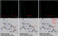
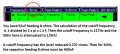
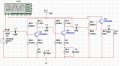
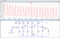
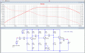
I am trying to build a multistage amplifier (CE>CE>CC) for delivering an average power of 200mW to an 8 Ohm speaker from a microphone that produces a 20 mV peak-peak sine wave. The source resistance is 500 Ohm. Lower cutoff frequency has to be below 50 Hz and upper cutoff has to be above 20 kHz. Attached is my current circuit. The gain from the CE stages is around 160 V/V, which is great, but when the CC stage is implemented the gain drops off to about 40 V/V and the upper and lower cutoff requirements can't be met. Any tips or suggestions would be greatly appreciated. I've tried bypassed and un-bypassed emitter resistances as well as different coupling capacitor values but nothing seems to get close to the requirements and still have a stable output on the oscilloscope. Thanks!
Attachments
-
 171.4 KB Views: 73
")