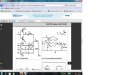
Hi, anyone how the switching on the right picture works? The paper mentions that the capacitors will converge to appropriately 1/3 and 2/3 after multiple DAC operation.
I want to know how can we do the switching of the voltage source Vb, Cbig1, Cbig2 and ground so that I can get the voltage at Cbig1 and Cbig2 to approach 2/3Vb and 1/3Vb.
By having that voltages at Cbig1 and Cbig2, we can do multi-step charging to save energy.
 Facebook
 Google
 GitHub
 Linkedin