Facebook
 Google
 GitHub
 Linkedin
Hello All,
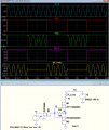
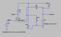
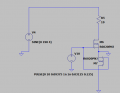
I do not understand why the MOSFET conducts for the negative cycle of applied input even though there's no voltage applied at the gate (PWM configured). Another thing why is the voltage at the point just above the MOSFET similar to input even though there's current flowing through the load. Shouldn't the voltage at that point be less than applied input because some voltage is dropping across the load? What am I missing?
I do not understand why the MOSFET conducts for the negative cycle of applied input even though there's no voltage applied at the gate (PWM configured). Another thing why is the voltage at the point just above the MOSFET similar to input even though there's current flowing through the load. Shouldn't the voltage at that point be less than applied input because some voltage is dropping across the load? What am I missing?
Attachments
-
 31.7 KB Views: 22
 -
 8.1 KB Views: 24
")