MOSFET IS BECOMING HOT WITHOUT LOAD

Thread Starter

ADI89

Joined Aug 13, 2013
10
HI,
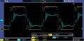
I have designed a full bridge DC DC converter by using Mosfet as switch. Mosfet Part no. stw22n95k5.All the four mosfet are mounted on one heat sink with proper isolation.
The switching frequency is 120Khz and DC input is 400V - 600 V.
I have used pulse transformer after the gate driver IC for driving both TOP and Bottom Mosfet.
Gate driver IC : ucc27324D
Pulse Transformer : GT03 111 069B
Gate resistance : 1 ohm to 47 ohm ( I have tried with different resistance)
Gate to source resitstance : 10 K

The heat sink is heating up even In no load condition also. After that I disconnected every thing and I gave the control supply to all four mosfet and incresed the DC input , still the heat sink is heating up.

I am not getting the problem for this . Please help me in this matter.
 

Thread Starter

ADI89

Joined Aug 13, 2013
10
Based on your word description, it should work. That's why we need a schematic of your circuit.
Now I am not using isolated feed back , directly i am giving the feedback to the controller from the secondary side. I have removed the CT from primary side and shorted. There is one capacitor in series with resistor connected from gate to source. Now that also i have removed. These are the changes i have done .

untitled_842x579.jpg
 

dannyf

Joined Sep 13, 2015
2,197
The heat sink is heating up even In no load condition also.
Switches don't dissipate much power if they are fully turned on / off. However, under light load, the incoming pulse may be too short to fully turn them on. The solution is to limit duty cycle or to use a beefier driver.

Similar things happened to a then "famed" and now forgotten Class D amplifier designer in the 1990s until I pointed that out to him - his amplifiers would work fine under heavy load but quickly burn up under no / light load.
 

Sensacell

Joined Jun 19, 2012
3,453
What is the bridge connected to?

Are there reactive currents flowing in some type of output filter?

Can you post more of the schematic?
 

ScottWang

Joined Aug 23, 2012
7,409
Some reasons may cause heat as:
1. High frequency oscillation.
2. Deadtime between up side mosfet and low side mosfet.
3. The rating wattage of mosfet is not enough.
4. Heatsink is too small.
If you have O'scope then you can measure the input/output waveform of mosfets bridge.
 

Thread Starter

ADI89

Joined Aug 13, 2013
10
Waveform 0039 :The yellow one is drain to source voltage of one mosfet and blue one is transformer primary current.

Waveform 0012 : The yellow one is gate to source voltage and blue one is drain to source voltage of same mosfet.

Both the waveforms are for same mosfet.
 

Attachments

ScottWang

Joined Aug 23, 2012
7,409
Did you compare the deadtime between up side mosfet and low side mosfet?
If the upper mosfet and lower mosfet turn on at the same time or very closely then the mosfet will heating up without load, during that time two mosfets will flow through a great current ad they will become two loads.
 

Thread Starter

ADI89

Joined Aug 13, 2013
10
Did you compare the deadtime between up side mosfet and low side mosfet?
If the upper mosfet and lower mosfet turn on at the same time or very closely then the mosfet will heating up without load, during that time two mosfets will flow through a great current ad they will become two loads.
I have given sufficient dead time. I have attached the waveforms (gate to source voltage) of both top and bottom Mosfet of same leg.
Zero Voltage time is the deadtime.
 

Thread Starter

ADI89

Joined Aug 13, 2013
10
Drain to source voltage pattern are coming different in different leg. The wave forms are given below.
Blue one : Drain to source voltage
Yellow : Gate to source Voltage
Actually the converter is a phase shifted Full bridge converter.
Is this reason for this difference in drain to source voltage waveform?
 

Attachments

Alec_t

Joined Sep 17, 2013
14,335
Those waveforms clearly show overlap of the pulse edges, i.e. apparently no dead-time. The upper and lower FET Vgs should have dead-time like this :-
DeadTime.PNG
 

kubeek

Joined Sep 20, 2005
5,795
Alec, I think you are looking at it wrong, you can see that there is a significant time where both gates are at 0V, and then one goes to +15V and the other to -15V i.e. one transistor goest on and the other stays off.
 
Top